
Cadence Design Systems

Automotive

Cadence Expands Tensilica Vision Family with Radar Accelerator and New DSPs for Automotive Applications - News
March 11, 2024Cadence Design Systems, Inc. expanded its Tensilica IP portfolio to address the increasing computational requirements associated with automotive sensor fusion applications. The new high-performance Cadence Tensilica Vision 331 DSP and Vision 341 DSP combine vision, radar, lidar and AI processing in a single DSP for multi-modal, sensor-based system designs, delivering energy efficiency in the small area.
Processing

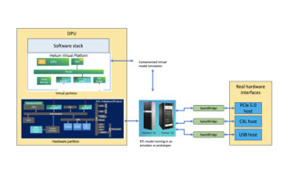
Spirent and Cadence Collaborate to Bring Advanced Chipset Testing to Pre-Silicon Verification - News
October 31, 2023CALABASAS, CA. – Spirent Communications plc announced a collaboration with Cadence Design Systems, Inc., to deliver a joint networking system-on-chip (SoC) verification solution that bridges to link the divide between pre-silicon and post-silicon verification.
AI & Machine Learning

Cadence's Neo NPU Comes out on TOPS - News
October 19, 2023San Jose. California. Cadence Design Systems introduced its innovative AI IP and software tools for on-device and edge AI processing. The scalable Cadence Neo Neural Processing Units (NPUs) support AI performance utilizing low energy while delivering up to 80 TOPS in a singular core. The NPUs offer both classic and new generative AI models for offloading AI/ML performance from any host processor (application processors, general-purpose microcontrollers, and DSPs) leveraging AMBA AXI interconnect.
Software & OS
The Appeal of Digital Twins Extends to Many Domains - Blog
September 20, 2023NASA pioneered the digital twin concept, from early space programs to the Mars Perseverance Rover. For NASA’s purposes, a twin on Earth can very accurately mimic a live remote craft.
Analog & Power
Optimizing PCB Design and Analysis for High-Speed Connector Interfaces - Whitepaper
June 13, 2023As high-speed connectors become more prevalent in various applications, PCB design teams face the challenge of optimizing the interface between high-speed connectors and PCBs with varying stack-ups and route densities, which can create crosstalk on high-speed signals.
Industrial

10X Faster Concurrent Full-Chip Optimization and Signoff from Cadence - News
October 18, 2022SAN JOSE, Calif. Cadence Design Systems, Inc. released its Cadence Certus Closure Solution for the automation and acceleration of a full design closure cycle (from signoff optimization through routing, static timing analysis (STA) and extraction) overnight. Benefits of the solution include: Innovative scalable architecture, Incremental signoff, Improved engineering productivity, SmartHub interface, 3D-IC design efficiencies.
Debug & Test

SEGGER and Cadence Add Native J-Link Support for Cadence Tensilica Cores - News
October 10, 2022Monheim am Rhein, Germany – October 10th, 2022 – SEGGER announced native J-Link debug probe support for select use cases with the Cadence Tensilica Processor IP. The Cadence Tensilica cores supported in the first implementation phase are the Tensilica Xtensa LX7 CPU, a number of Tensilica HiFi DSPs (HiFi 4, HiFi 3z, HiFi 3, and HiFi 1), and also the Tensilica Fusion F1 DSP.