The Morphing of Electronic Product Design in the Era of Moore's Law 2.0
April 20, 2020
News
The original Moore's Law was all about tracking the number of transistors that could be packed into a dense integrated circuit. It was an observation, not a law of physics.
The original Moore’s Law was all about tracking the number of transistors that could be packed into a dense integrated circuit. It was an observation, not a law of physics, that tracked the progress in semiconductor process development and manufacturing.
From the consumer viewpoint, Moore’s Law is associated with a continuing evolution of products that provide more functionality, deliver more performance, use less energy, and in many cases, are smaller. The laws of physics do apply to semiconductor processing and manufacturing. In fact, the rate of progress in transistor size and chip density has slowed down.
This doesn’t mean that we are done delivering innovative products that continue to add expanded functionality and performance. Moore’s Law 2.0 is a recognition that there are other ways to continue that go beyond the simple metric of transistor density on the wafer.
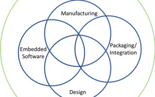
Moore’s Law 2.0 is not about increasing transistor counts and densities. It’s about measuring the progress in our ability to continue to deliver innovative electronic products and systems. This is happening with many drivers in the transformation to 2.0 and many things that come together to make an innovative electronic product possible. These include semiconductor manufacturing processes, including new materials and structures, advanced design automation and verification tools, and availability of a wide array of semiconductor intellectual property. Other drivers are embedded software development and debugging platforms and advanced packaging technologies that include two- and three-dimensional structures, flexible substrates, and materials.
Together contributions in these areas are driving Moore’s Law 2.0
It’s playing out in the design ecosystem as well. During the heyday of Moore’s Law, the items in the list above were generally viewed as discrete and separate activities in the product manufacturing chain. Chip design teams focused their energies on achieving chip tape out, the key milestone for release of a new design to manufacturing. During this period of time, the team was comprised primarily of chip design and verification engineers. While communication with the groups responsible for packaging design, software design and system integration occurred, these were typically separate groups and often in a different part of the organization.
The era of Moore’s Law 2.0 is upending this “siloed” approach to product design. Developing a successful new electronic product requires the various stakeholders to be aligned on the same team from the beginning. Each contributes to one or more dimension of the features that will enable the product to meet its target specifications. In the past era, semiconductor process and manufacturing technology improvements were the key driver for higher performance, lower power and greater functional density. In the 2.0 era, this is no longer the case as each element of the team has important contributions to make.
Consider the role of the embedded software development team. Without embedded software, the chip or SoC is just a big collection of transistors. It needs software that defines the functions of the device in terms of its intended application. If the application requires low power, the software team and chip design team working together can achieve lower-power targets by leveraging both the hardware architecture of the chip and the software that controls it. Today’s smartphones are a good example of how clever chip and software design extend the battery life of these mobile computing platforms.
Continuing this same thread, imagine what a smartphone would look like if a packaging and system integration team wasn’t involved in the product design from the beginning. There are many tradeoffs to consider in terms of making the product as compact as possible. These tradeoffs directly affect chip layout and package design, interconnect and form factor. Additional considerations include heat management, mechanical stress, and overall durability.

Without question, we are witnessing a major shift in our industry as once separate functions are coming together to deliver the products of the future. Chip design, semiconductor processing technology, software development, packaging, interconnect and even mechanical and thermal design are all coming together to work on what we now refer to as electronic system design.
Organizations had to change too. The ESD Alliance began life as EDAC (Electronic Design Automation Consortium) in 1989. As the name suggested, it was focused on the emerging market for design automation tools. Through the 90s and first decade of the 21st century, our industry was driven by Moore’s Law and EDAC’s member community was driven by advances in EDA and verification.
In 2017 and in recognition of the shift to Moore’s Law 2.0, EDAC changed its name and expanded its mission to Electronic System Design Alliance. Our mission and becoming a SEMI Strategic Technology Community representing members in the electronic system and semiconductor design ecosystem better aligns us with the shift from a chip-design centric worldview to electronic system design and beyond. Indeed, interest in electronic system design is growing from the manufacturing community. We’re responding through the global SEMICON events, including a well-attended Design Council Meeting during SEMICON Taiwan last year.
For more information, visit the ESD Alliance website.
About the Author
Robert (Bob) Smith is Executive Director of the ESD Alliance, a SEMI Strategic Association Partner. He is responsible for the management and operations of the ESD Alliance, an international association of companies providing goods and services throughout the semiconductor design ecosystem.