Flexibility to update firmware, a key to IoT devices
April 13, 2017
Blog

Internet of Things (IoT) devices are being introduced into the market at a rapid pace – from home appliances to medical devices to cars – as manufacturers must stay ahead of their competitors...
Internet of Things (IoT) devices are being introduced into the market at a rapid pace – from home appliances to medical devices to cars – as manufacturers must stay ahead of their competitors with new innovations and the flexibility to adopt or integrate new technologies. Designers must build flexibility into their products to meet the evolving IoT ecosystem as new functionalities and regulations are adopted. Firmware updates not only allow customization during initial deployment at a customer site, but also enable new functions/features to be added after a product has been in the field or allows fixing of any firmware issues during usage.
Non-volatile memory (NVM) devices such as NOR flash are commonly used as a firmware code storage medium due to their reprogrammability and reliability. By rewriting a portion of the device firmware code residing in the NVM used in the device, manufacturers can easily update device capabilities.
When looking to update firmware there are three things to consider:
- What/how much code to update
- How often to update
- The time it will take (speed) to perform the update
What/how much firmware code to update
What and how much firmware code to update must be considered during the initial design phase of the IoT device. The updatable portion of the firmware must be stored in separate area of the NOR flash device than the non-updatable portion.
Updating any piece of NOR flash starts with first erasing that portion of the memory and then programming new information into that portion. NOR flash is organized in portions of different sizes called sectors and blocks. NOR flash devices, such as SST’s 64 Mb SuperFlash SST26VF064B technology are organized in uniform 4 KB sectors (4 KB = 4 * 1024 * 8bits = 32,762 bits) that can individually be erased and reprogrammed. They can also be organized in larger 8 KB, 32 KB, and 64 KB blocks that can also be individually erased. Thus, one 8 KB block has two sectors, one 32 KB block has eight sectors, and one 64 KB block has 16 sectors. Figure 1 shows the memory organization of the SST26VF064B in 8/32/64 KB blocks, each of which can be individually protected.

[Figure 1 | Memory organization (map) of the SST26VF064B, which consists of eight 8 KB blocks, two 32 KB blocks, and 126 64 KB blocks. Click to zoom.]
Prior to performing any update to any portion of the flash, blocks in that portion must be unprotected to allow for erasing and programming. After completing an update it is prudent to again protect those blocks to prevent any inadvertent writing or erasing of those areas.
The updatable portion of the firmware must be organized in sectors and blocks in such a manner that there is enough flexibility to allow both limited and maximum feature/function updates. Since the speed of an update is determined by the number of sectors and blocks that need to be erased and re-programmed, it is better to think of speed and flexibility together when organizing the updatable portion of the firmware. Figure 2 shows an example of organizing the memory into updatable and non-updatable portions. Non-updatable portions (such as boot code) are stored in protected regions, while updatable portions of firmware (such as features/functions) are divided into smaller or larger blocks based on flexibility requirements. Updatable image files are stored in larger blocks and updatable variables/parameters are stored in smaller blocks.
 [Figure 2 | Organizing memory in non-updatable portions (such as boot code) and updatable portions (such as code for functions/features, image files, and parameter variables). Click to zoom.]
How often to update
The main limitation to how often you may want to update firmware is the endurance limitation of the memory used in an application. SuperFlash technology memory such as the SST26VF064B has 100,000 endurance cycles, which means that each sector can be programmed and erased 100,000 times. The possibility of updating firmware 100,000 times sounds like plenty; however, many IoT devices collect data and store the information in NOR flash during operation so this must be considered when calculating maximum endurance cycle limitations.
It is also important to allocate sufficient sectors in the memory to account for endurance. For example:
Suppose the IoT device is collecting and storing 16 bytes of information and the information is expected to be collected and stored 100 million times during the life of the product. The number of sectors that should be allocated can be calculated as follows:
1 sector = 4 KB
Assume all the address locations in the sector are used to store information, 16 bytes of data at a time, and are written to a new address location until the end of the sector is reached (e.g., 0×0000-0x000F then 0×0010-0x001F then 0×0020-0x002F, etc.).
Since 4 KB/16 bytes = 256, that is the number of times storage can be written before reaching capacity in the sector and erasing any data in the sector. If the endurance limit of one sector is 100,000 cycles, and one sector can be written 256 times for 100,000 cycles, data can be collected and stored 25,600,000 times.
If an application requires data be collected and stored 100 million times, the number of sectors to allocate is calculated as 100,000,000/25,600,000 = 3.9. Therefore, in this example, it is necessary to allocate 4 sectors to store 16 bytes of data for the life of the application.
IoT device engineers need to do similar calculations to allocate sufficient sectors and blocks for data logging parameters so as not to breach the endurance limit of their NOR flash device.
Speed of updates
The speed of an update can be calculated based on the number of blocks and sectors that need to be erased and reprogrammed. Suppose it is necessary to reprogram 1 Mb, 2 Mb, or 4 Mb of firmware code/data stored in several 64 KB blocks in an SST26VF064B. The code/data can be comprised of firmware code, image files, or other code that needs to be updated. Doing the update involves performing a sequence of command instructions to flash. The sequence would start with unprotecting the blocks of memory, erasing those blocks, programming those blocks with updated data/code, and re-protecting those blocks of memory.
For the SST26VF064B, the required sequence of instructions for updating 1 Mb, 2 Mb, or 4 Mb of memory is shown in Table 1. From Table 1 it is evident that the two most significant periods are erase time and program time.

[Table 1 | Sequence of flash command instructions to update 1 Mb, 2 Mb, or 4 Mb of memory. Click to zoom.]
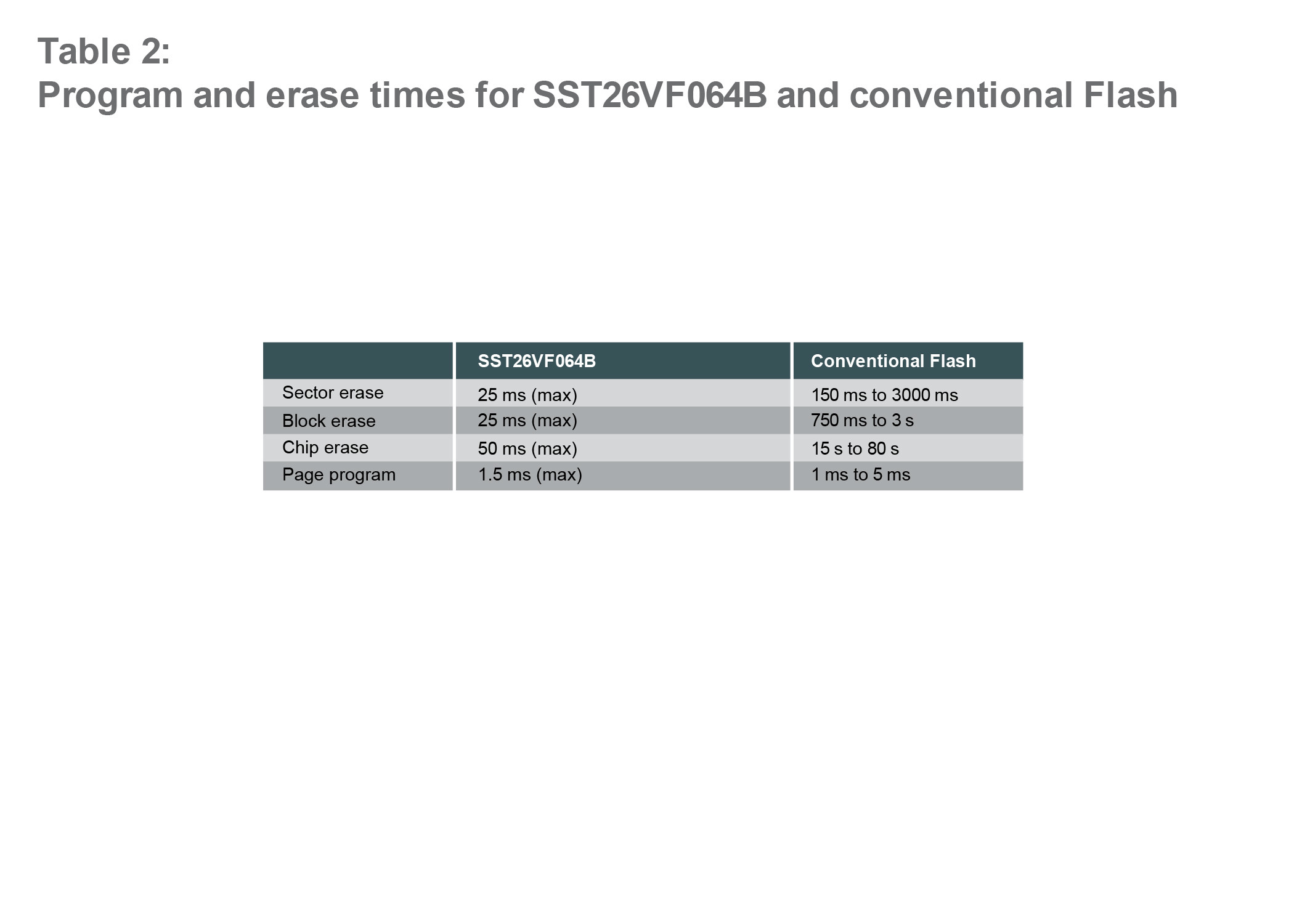
The SST26VF064B uses SuperFlash technology, which provides excellent erase performance. A comparison of erase and program performance for SuperFlash technology versus conventional flash is shown in Table 2. The vastly superior erase performance provided by SuperFlash technology as compared to conventional flash is immensely useful for reducing update time. The SST26VF064B supports a maximum clock frequency of 104 MHz, maximum sector erase time of 25 ms, maximum block erase time of 25 ms, and maximum page program time of 1.5 ms. A 12 ns delay (CE high time) is also required between each command instruction to flash memory operating at a clock frequency of 104 MHz.

[Table 2 | Program and erase times for the SST26VF064B and conventional flash. Click to zoom.]
Using the sequence of commands shown in Table 1, along with knowledge of the program and erase times, the calculation for the amount of time required to update 1 Mb, 2 Mb, or 4 Mb of SuperFlash technology memory and conventional flash memory is shown in Tables 3 and 4, respectively. Such calculations must be done by IoT device engineers to estimate the speed of doing updates with the aim of minimizing the IoT device downtime during updates.

[Table 3 | Amount of time required to update 1 Mb, 2 Mb, or 4 Mb of SuperFlash technology memory. Click to zoom.]

[Table 4 | Amount of time required to update 1 Mb, 2 Mb, or 4 Mb of conventional flash memory. Click to zoom.]
Conclusion
IoT device design engineers need to provide the flexibility to update application code and data. What and how much code to update, how often to update, and the speed of updates are issues that need to be addressed while designing an IoT device. The selection of NVM impacts these issues and plays a critical role in calculating the timing and speed of code updates.
Microchip Technology, Inc.
LinkedIn: www.linkedin.com/company-beta/6481/
Facebook: www.facebook.com/microchiptechnology
Google+: plus.google.com/+MicrochipTech


