PCB Materials and Design Requirements for 5G Products
July 22, 2021
Story
PCBs are the heart of every electronic product. They not only facilitate electrical connections between components but also transmit signals of all sorts and electric currents. With the invention of 5G technology, what are the materials and design requirements that circuit boards must meet?
Unlike 4G, the deployment of 5G systems will compel designers to consider the designs of printed circuit boards for smartphones, the internet of things, and telecommunications gadgets. Since the 5G systems require high transmission speeds, extensive bandwidths, and minimal latencies, designers must proceed with high precision to meet those requirements.
5G Design Requirements
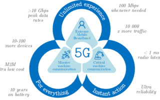
If you compare and contrast the various networking requirements, you will get scattered and conflicting information from different locations. The world is expecting 3 billion extra mobile and IoT products before the end of this year. 5G products aim to offer 10-20 times faster data rates – almost 1000 times more traffic and ten times as many links per kilometer square than their 4G counterparts. In addition, 5G aims to offer a latency of 1 ms – 10 times the 4G network latency.

(Image source)
5G systems will also work at higher frequencies than 4G and 3G systems. Therefore, circuit boards for mobile and networking gadgets must support higher digital data rates and frequencies. This will stretch diverse signal designs to full capacities. Remember, 4G systems function at frequencies of 600MHZ-5.925GHZ. Their 5G counterparts extend the higher frequency levels to mm-waves.
Designers should also consider the bandwidth per station when creating wireless communication capacities in 5G network boards. The station bandwidth in 4G is 20 MHz, and 100 MHz for 5G products. The existing ICs can support the stretched frequencies and speeds in 5G products, but board materials will significantly determine their performance.
Choosing PCB Materials for 5G Systems
As seen from the above discussion, designing for 5G products requires high-frequency diverse signals. Besides the typical high-speed design and high-frequency layout guidelines, using the appropriate PCB materials can inhibit signal losses and ensure excellent signal quality. Since 5G products use mixed signals, designers should deter electromagnetic interference between analog and digital PCB parts and design their PCBs to FCC EMC standards.
In preparation for the high demand that lies ahead, PCB substrate manufacturers have started creating materials with low dielectric constant compared to standard FR4 materials. Even with higher frequencies, these new 5G materials display minimal losses than PTFE materials.
Boards for 5G products require processors and amplifiers that perform at high speed and high frequency. You can reduce the output disparities in these components using heat management. The heat transmission and heat coefficient are essential substrate factors in 5G products. The heat produced by the PCB operation can cause an increase in temperature, leading to a reduction in dielectric performance slowly.
The benefit of the first aspect is understandable: a material with high heat transmission capacity effectively conducts temperature away from the source. It is an excellent choice for applications with high speeds and frequencies. On the other hand, the benefits of the thermal coefficient factor are not obvious. Dielectric constant variations can cause distribution along an intersection. High distribution can create signal echoes along a conduction line in rare instances.
Regardless of the material you will use to design a PCB for a 5G application, you must adhere to the standard circuit board design practices to achieve constant impedance throughout the intersects. For instance, you should route the traces of RF signal lines with an express track. Additionally, you should tightly regulate the conductor measurements to produce constant impedance. The other general PCB design guidelines you should remember are:
- Applying less solder mask: Since most solder masks display high water absorption capacity, the use of more solder mask will cause more moisture absorption, causing high dielectric losses.
- Using smooth and regular traces: The standard skin depth is indirectly relative to the frequency. Thus, it will be pretty shallow on a high-frequency board. A rough surface will create a rough track, raising the resistive damages.
- Using substrates with minimal Dk values: The Dk value increases consistently with the frequency. Therefore, it is advisable to pick substrates with minimal Dk values.
Conclusion
PCB designers and component manufacturers must prepare for the coming 5G revolution. Considering the points we have discussed above, they will be on the right track and reap big from the high demand for high-frequency boards and components.
Linda Liu is the overseas marketing manager for MKTPCB, a leading PCB manufacturer that offers high-quality PCB products and services. Since 2012, she has established “first-of-its-kind” industry-changing and transformational businesses initiatives that increased revenue growth, brand exposure and market expansion for MKTPCB. Linda graduated from Western University with a bachelors degree in marketing.

Linda Liu is the overseas marketing manager for MKTPCB, a leading PCB manufacturer that offers high-quality PCB products and services. Since 2012, she has established “first-of-its-kind” industry-changing and transformational businesses initiatives that increased revenue growth, brand exposure and market expansion for MKTPCB. Linda graduated from Western University with a bachelors degree in marketing.