Using Safety Application Notes to Aid Safety Designs—Part 3: Improving Functional Safety Performance
May 11, 2026
Blog

After doing a first iteration of the failure modes, effects, and diagnostics analysis (FMEDA) on a safety function’s circuit, there can only be two outcomes. The first is that the system integrity level (SIL) requirements are achieved, and the second is a failure to meet the requirements.
To address the latter without having significant architectural changes, system integrators can either increase the diagnostic coverage, adjust the operating conditions, and/or employ additional safety measures. Analog Devices’ safety application notes contain information that can help system integrators make such design improvements to achieve the required probability of dangerous failure per hour (PFH)/probability of dangerous failure on demand (PFDAVG) and safe failure fraction (SFF). For this reason, this third part of the series provides insights on how system integrators can use a functional safety (FS)-enabled part’s safety application note to improve the IC’s functional safety performance in the system.
An Example FMEDA
Part 2 of this series showed how system integrators can use a functional safety (FS)-enabled part’s safety information contained in the IC’s safety application note when doing the system failure modes, effects, and diagnostics analysis (FMEDA). After performing a first run of the FMEDA, if the safety function’s design already has a good architecture for FS, it may already achieve its required average frequency of dangerous failure per hour (PFH)/average probability of dangerous failure on demand (PFDAVG) and safe failure fraction (SFF) requirements. Otherwise, it will need further design improvements.
As an example, Table 1 shows a system FMEDA that focuses on the ADP7156’s impact on an assumed single-channel (no hardware fault tolerance (HFT)/HFT = 0) safety function. For the analysis, it is assumed that:
- The LDO provides power to a logic controller.
- The safe state of the safety function can be achieved if the output voltage of the low dropout (LDO) is at 0V; otherwise, the effect can either lead to no effect on the safety function or loss of the safety function.
For the diagnostic, the assumption is that the technique overvoltage protection with safety shutoff is used (see IEC 61508-2:2010 Table A.9) so that a 60% maximum claimable diagnostic coverage (DC) can be achieved for dangerous failures pertaining to overvoltage. In terms of operation, the safety function is assumed to operate in high-demand mode. Similarly, the failure rate prediction used for this article is by IEC 62380.
Table 1. Example FMEDA Focused on the ADP7156
|
Name |
Component |
Function |
Failure Rate |
Failure Mode |
FMD (%) |
Effect |
Failure Classification |
DC (%) |
λS (FIT) |
λNE (FIT) |
λDD (FIT) |
λDU (FIT) |
|
IC1 |
LDO regulator |
Provide low-noise, regulated voltage output of 3.3V ± 1.5% within 1.2ms after enable |
7.15 FIT |
VOUT is off or stuck low close to 0V |
29 |
Safety function at safe state |
Safe |
— |
2.07 |
|
|
|
|
VOUT regulates higher than target |
12 |
Loss of safety function due to damaged controller |
Dangerous |
60 |
|
|
0.52 |
0.34 |
||||
|
VOUT regulates lower than target |
9 |
Loss of safety function |
Dangerous |
0 |
|
|
|
0.64 |
||||
|
VOUT output is oscillating but within regulation |
6 |
No effect on safety function |
No effect |
— |
|
0.43 |
|
|
||||
|
VOUT is stuck close to VIN |
24 |
Loss of safety function due to damaged controller |
Dangerous |
60 |
|
|
1.03 |
0.69 |
||||
|
VOUT settling time > 1.2ms |
3 |
No effect on safety function |
No effect |
— |
|
0.21 |
|
|
||||
|
VOUT output is oscillating but outside regulation |
1 |
Loss of safety function due to damaged controller |
Dangerous |
60 |
|
|
0.04 |
0.03 |
||||
|
No effect on system function |
16 |
No effect on safety function |
No effect |
— |
|
1.14 |
|
|
||||
|
0.39 FIT |
VOUT is off or stuck low close to 0V |
32.2 |
Safety function at safe state |
Safe |
— |
0.13 |
|
|
|
|||
|
VOUT regulates higher than target |
6.8 |
Loss of safety function due to damaged controller |
Dangerous |
60 |
|
|
0.02 |
0.01 |
||||
|
VOUT regulates lower than target |
6.8 |
Loss of safety function |
Dangerous |
0 |
|
|
|
0.03 |
||||
|
VOUT output is oscillating but within regulation |
3.4 |
No effect on safety function |
No effect |
— |
|
0.01 |
|
|
||||
|
VOUT is stuck close to VIN |
20.5 |
Loss of safety function due to damaged controller |
Dangerous |
60 |
|
|
0.05 |
0.03 |
||||
|
No effect on system function |
30.3 |
No effect on safety function |
No effect |
— |
|
0.12 |
|
|
||||
|
Total |
2.2 |
1.91 |
1.66 |
1.77 |
||||||||
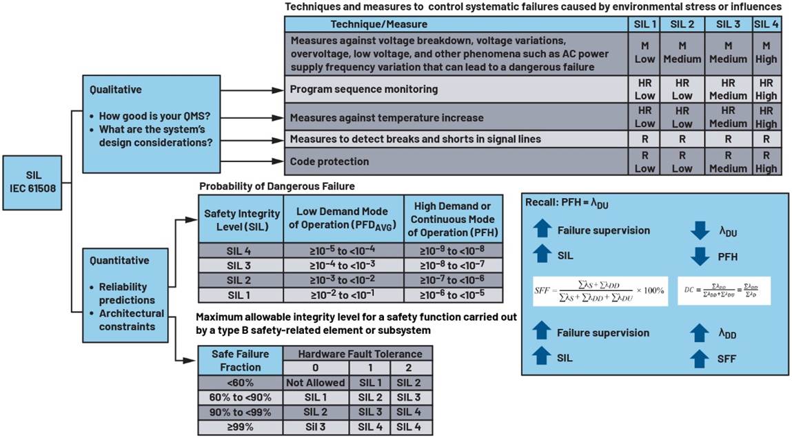
Figure 1. Diagnostics through the lens of IEC 61508:2010.2
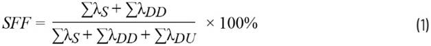
Recall to calculate SFF1:
To calculate the IC’s average frequency of dangerous failure per hour (PFH)1:

With the current design, the SFF of the safety function is 69% while the PFH contribution is 1.77FIT. If the safety function needs to achieve system integrity level (SIL) 2 according to IEC 61508, the design will need to have an SFF of at least 90%. Meanwhile, the SIL 2 allowed PFH is from 100FIT to 1000FIT. Assuming 1% of the PFH is allocated to the IC, the required PFH contribution will be in the range 1FIT to 10FIT. If the target is the lower limit or 1FIT, then the current architecture will not comply with the SFF and PFH requirements for SIL 2.
With this, the following sections show how system integrators can improve their design’s PFH and SFF metrics.
Improving the Diagnostic Coverage
Equation 2 showed that PFH is directly proportional to the dangerous-undetected failure rate. Similarly, Equation 1 showed that SFF is directly proportional to the safe and dangerous-detected failure rates. Therefore, lowering the dangerous-undetected failure rate and increasing the dangerous-detected one will improve both the PFH and SFF metrics of the IC. This is shown in Figure 1.
In the case of the FMEDA example shown in Table 1, only the overvoltage-related failures have diagnostic coverage. To improve the IC’s safety performance, there are two ways related to increasing diagnostic coverage. The first one is by adding diagnostic coverage to detect undervoltage-related dangerous failures, while the second one is increasing the diagnostic coverage for the overvoltage-related dangerous failures; for example, DC increases from 60% to 90%.
The current design uses an overvoltage protection with a safety shutoff diagnostic measure, which IEC 61508-2:2010 table A.9 states, with a maximum claimable diagnostic coverage of 60%. Using the voltage control (secondary) diagnostic measure to monitor the output of the ADP7156 will provide a maximum claimable DC of 99%. Since such a diagnostic measure monitors both overvoltage (OV) and undervoltage (UV) or any abnormality outside a specified range, the OV- and UV-related dangerous failures will be covered. Applying this to the example FMEDA as in Table 2, a PFH of 0.04FIT and SFF of 99.3% can be achieved, exceeding the SIL 2 requirements.1,3
Optimizing the Reliability Predictions
Another way to improve the PFH of an IC is by lowering its estimated failure rate. Part 1 of the Know Your Safety Application Notes series showed how system integrators can calculate an FS-enabled part’s failure rate based on high-temperature operating life (HTOL), SN 29500, and IEC 62380. With the assumed conditions given in ADI’s safety application notes, system integrators can use the information provided to ensure the reliability predictions match their operating conditions rather than using worst-case values.
For example, the ADP7156’s reliability prediction according to SN 29500 FIT with its assumed operating conditions is shown in Figure 2. Since the SN 29500 reliability prediction is affected by application-related parameters such as the voltage dependence factor and the temperature dependence factor, designers can tailor the assumed IC’s operating conditions like operating voltage, ambient operating temperature, mission profile, and loading conditions, to match theirs if the assumed ones appear worse than their actual application.
Table 2. Example FMEDA Focused on the ADP7156
|
Name |
Component |
Function |
Failure Rate |
Failure Mode |
FMD (%) |
Effect |
Failure Classification |
DC (%) |
λS (FIT) |
λNE (FIT) |
λDD (FIT) |
λDU (FIT) |
|
IC1 |
LDO regulator |
Provide low-noise, regulated voltage output of 3.3V ± 1.5% within 1.2ms after enable |
7.15 FIT |
VOUT is off or stuck low close to 0V |
29 |
Safety function at safe state |
Safe |
— |
2.07 |
|
|
|
|
VOUT regulates higher than target |
12 |
Loss of safety function due to damaged controller |
Dangerous |
99 |
|
|
0.85 |
0.01 |
||||
|
VOUT regulates lower than target |
9 |
Loss of safety function |
Dangerous |
99 |
|
|
0.63 |
0.01 |
||||
|
VOUT output is oscillating but within regulation |
6 |
No effect on safety function |
No effect |
— |
|
0.43 |
|
|
||||
|
VOUT is stuck close to VIN |
24 |
Loss of safety function due to damaged controller |
Dangerous |
99 |
|
|
1.7 |
0.02 |
||||
|
VOUT settling time > 1.2ms |
3 |
No effect on safety function |
No effect |
— |
|
0.21 |
|
|
||||
|
VOUT output is oscillating but outside regulation |
1 |
Loss of safety function due to damaged controller |
Dangerous |
99 |
|
|
0.07 |
0.00 |
||||
|
No effect on system function |
16 |
No effect on safety function |
No effect |
— |
|
1.14 |
|
|
||||
|
0.39 FIT |
VOUT is off or stuck low close to 0V |
32.2 |
Safety function at safe state |
Safe |
— |
0.13 |
|
|
|
|||
|
VOUT regulates higher than target |
6.8 |
Loss of safety function due to damaged controller |
Dangerous |
99 |
|
|
0.03 |
0.00 |
||||
|
VOUT regulates lower than target |
6.8 |
Loss of safety function |
Dangerous |
99 |
|
|
0.03 |
0.00 |
||||
|
VOUT output is oscillating but within regulation |
3.4 |
No effect on safety function |
No effect |
— |
|
0.01 |
|
|
||||
|
VOUT is stuck close to VIN |
20.5 |
Loss of safety function due to damaged controller |
Dangerous |
99 |
|
|
0.08 |
0.00 |
||||
|
No effect on system function |
30.3 |
No effect on safety function |
No effect |
— |
|
0.12 |
|
|
||||
|
Total |
2.2 |
1.91 |
3.39 |
0.04 |
||||||||
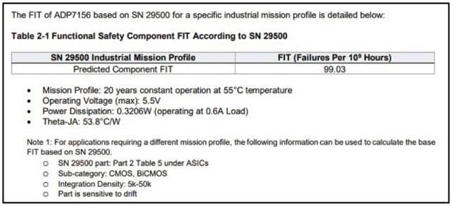
Figure 2. ADP7156’s SN 29500 FIT based on its Safety Application Note.
Employing Additional Safety Measures
ADI’s safety application notes also show the assumed application circuit used in the analysis as shown in Figure 3. Alongside the system failure modes provided in the failure mode distribution (FMD) section of the application note, designers will be able to decide how to address such failure modes with additional safety measures if needed. For instance, a protective measure such as a Zener diode and a fuse can be added for the output’s OV-related dangerous failures. With such protection, the Zener diode will clamp the overvoltage to make such failure no-effect, eliminating dangerous failures, thus improving PFH and SFF metrics.
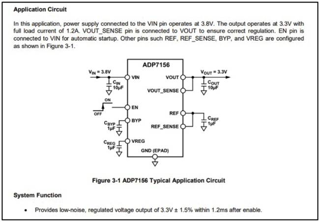
Figure 3. ADP7156 assumed application circuit in its safety application note.
Conclusion
Achieving stringent SIL requirements does not always necessitate a complete overhaul of a system’s architecture; rather, it often requires a strategic refinement of the existing design using targeted diagnostic and reliability data. By leveraging the insights provided in Analog Devices’ safety application notes, system integrators can systematically improve functional safety performance—specifically the SFF and PFH/PFDAVG—through the enhancement of diagnostic coverage, the optimization of operating conditions to lower the estimated failure rates, or the integration of supplemental safety measures like external protection circuits. As demonstrated with the ADP7156 LDO regulator, transitioning from basic overvoltage shutoff to secondary voltage monitoring can dramatically shift a design from non-compliance to exceeding SIL 2 standards. Ultimately, these application notes serve as a critical roadmap for engineers to aid their safety designs, ensuring that integrated circuits meet the rigorous demands of IEC 61508 with precision and efficiency.
References
1Bryan Borres. ”Know Your Safety Application Notes—Part 2: Failure Mode Distribution.” Analog Dialogue, Vol. 59, October 2025.
2Bryan Borres. ”Improving Industrial Functional Safety Compliance with High Performance Supervisory Circuits: Using SIL-Rated Components—Part 2.” Analog Devices, Inc., March 2025.
3Bryan Borres and Noel Tenorio. “Designing Power Supplies for Industrial Functional Safety—Part 1: What IEC 61508 Tells Us.” Analog Devices, Inc., July 2025.

Bryan Angelo Borres is a TÜV-certified functional safety engineer who focuses on industrial functional safety. As a senior functional safety engineer, he helps component designers and system integrators design functionally safe power products that comply with industrial functional safety standards such as the IEC 61508. Bryan is a member of the IEC National Committee of the Philippines to IEC TC65/SC65A and IEEE Functional Safety Standards Committee. He also has a postgraduate diploma in power electronics and more than seven years of extensive experience in designing efficient and robust power electronics systems.