Guidelines for designing a printed circuit board
September 08, 2017

Designing a circuit board is both an art and science. So what?s needed to ensure a perfect design? I?ll lay it out here in five steps.
Designing a circuit board is both an art and science. So what’s needed to ensure a perfect design? I’ll lay it out here in five steps.
First, paying attention to PCB design is crucial for avoiding problems later. Creating a PCB is like conceiving the digital image and translating it into a physical entity. Thus, the circuit board design needs to be realistic enough to put on paper and convert into a tangible form.
1. Refine the component placement plan
While a PCB is not as vast as a landscape, you’re given a challenge to do wonders on a small piece of metal board. So, it’s important to ensure that the component placement plan is repeatedly revised to achieve the best use of the PCB. Hence:
- Pay attention to orientation: As a general rule, your PCB design should have similar components placed in a common orientation. This helps a lot during the soldering process, and errors are reduced.
- Determine correct placement: The components shouldn’t be placed on the solder side of the board.
- Choose fool-proof organization. All surface-mount components should be placed on the same side of the board, and through-hole components are generally fit on the top side of the board. This enables quick assembling.
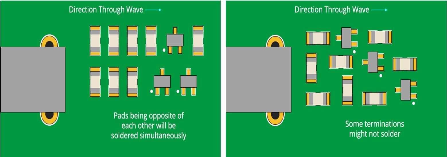
[Figure 1 | Shown is proper chip orientation (left) verses poor orientation (right).]
2. Placement of ground, signal, and power traces
A PCB must be designed so that the signals have a clear pathway across all the placed components. This is ensured by proper power- and ground-plane orientation; connecting the signal traces as per the schematic guidelines; and ensuring optimal net widths.
First, experts recommend that the power and ground planes should be internal to the board, and these should be both centered and symmetrically placed. This keeps the board from bending in addition to supporting the correct component placement. Common rails should be made for the supply route and the traces should be firm and wide. Daisy-chaining power-lines end-to-end should be avoided.
Second, if a horizontal trace is carved due to a component’s placement on one side of the board, then the traces should run vertically on the opposite side. Moreover, the traces should be short and direct and should be in the space between the components.
And third, though the amount of current passing through the design determines the net width, it’s still stipulated that a 0.010-in. width is ideal for low current analog and digital signals. Net width must be wider if the traces carry current more than 0.3 A.
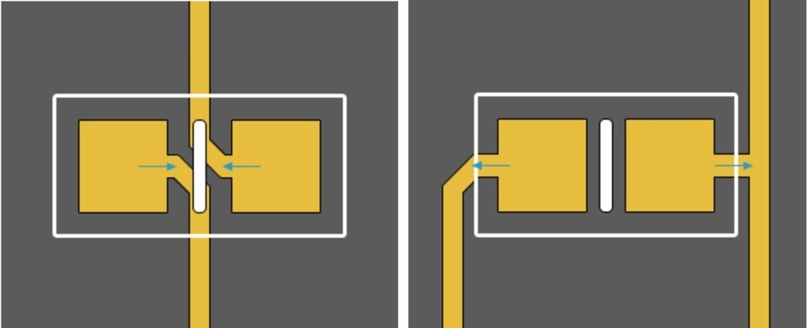
[Figure 2 | Preferred routing is indicated by the arrows in the solder migration.]
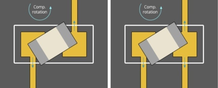
[Figure 3 | Shown here are non-preferred routing signals.]
3. Keep things separate
It’s a common observation that large voltage supplies and current spikes interfere with circuits that require low voltage and smaller currents. These interference issues can be best dealt with:
- Separation of power and control ground for every power supply stage. In they need to be tied together, do so at the end of the supply path.
- If the ground plane is placed in the middle layer, then a small impedance path should be created to reduce the interference risk and also to protect the control signals. The digital and analog grounds are separated using the same procedure.
- Capacitive coupling is likely to occur when the large ground plane is crossed by lines on both sides. Avoid this by only allowing analog signals to pass through the analog ground. In four-layer PCB design, this is more critical.
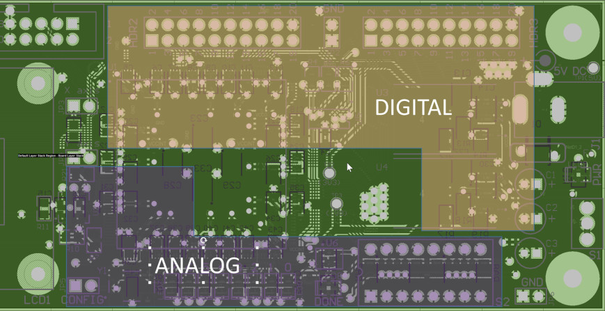
[Figure 4 | Proper component separation can be seen here.]
4. Tackling the heat
A board can be damaged by excessive heat. Hence, heat-dissipation methods should be adopted, including finding the casual components and adding thermal reliefs. To Schieve the former, use components that have optimal thermal resistance ratings. Cooling fans and heat sinks (preferred) can be added. Any critical components should be kept away from the heat source.
Thermal reliefs are useful for wave soldering on assemblies with high copper content or multiple-layers boards. These reliefs should be used on through-hole components to ease the soldering process and avoid the heat build-up in the component plates. To minimize mechanical and thermal stress, add teardrops at points where traces join pads.
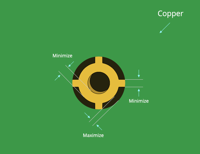
[ Figure 5 | This is a typical thermal relief pattern.]
5. Recheck everything
You might feel like you’ve created a master-piece, but such thoughts shouldn’t stop you from checking and re-checking the final configurations. Perform an Electrical Rules and Design Rules check to verify that all the rules are conformed to. Then, check to be sure that all recommended signal routing is in place and look for any lapses.