Using NOR and NAND flash memory in M2M applications
March 01, 2014
Machine-to-Machine (M2M) devices are requiring more memory capacity, which has many evaluating NOR and NAND flash-based solutions. Designers need to c...
Expanding M2M capabilities and solutions enable new products and services that are transforming the way we work and play. M2M solutions are available in several form factors and radio interfaces, but are most commonly sold in module form – discrete or mounted on a PCB. Embedded memory typically enables short-range radio solutions (Wi-Fi, ZigBee, Z-wave, Bluetooth, IP500). Usually, the memory subsystem – in terms of embedded flash and RAM – is contained on the processor. If the memory cannot be placed on the processor, low-density, external NOR flash memory or RAM may be added.
While many short-range M2M wireless solutions are sufficient for consumer-centric applications (like appliance connectivity and home automation), infrastructure and mission-critical applications (health, safety, automobiles, retail, and smart city applications) require robust and always-on cellular network connectivity. In long-range radio solutions like cellular M2M, it is not cost-effective to embed a high-density memory device on the processor chip, so critical communication code must be managed in the external flash memory and RAM. Figure 1 shows a typical cellular M2M module, including a software stack.
|
|

M2M cellular modules are available in 2G and 3G/4G versions. On GSM networks, GPRS and EDGE are considered 2G, and on CDMA networks, 1xRTT (or CDMA2000) is considered 2G. 3G networks are based on the global High-Speed Downlink Packet Access (HSDPA) standard, which is compatible with common Microprocessor Unit (MPU) architectures and enables rich, real-time multimedia and browsing experiences. Automotive infotainment, transportation, and video surveillance services are driving higher bandwidth requirements that are only available on 3G and 4G networks.
As the revenue and capacity of data services exceed traditional voice services, Mobile Network Operators (MNOs) who are deploying billion dollar, revenue-generating M2M services have every incentive to leverage 3G and 4G networks in order to utilize network resources and finite spectrums most efficiently. AT&T has already announced plans to take 2G networks offline in the United States by 2017, and leading M2M module suppliers are excluding 2G-certified modules from new designs[1]. 2G M2M solutions are also reliant upon legacy component support and manufacturing assets that are starting to become obsolete. These factors have helped to position 3G M2M modules in the sweet spot of market growth – with $5 billion in 3G and 4G M2M connections forecasted to come online over the next four years[2].
Cellular M2M memory requirements: Small form factor
2G M2M modules have modem speeds up to 130 Kbps and use NOR flash memory with critical communication code storage requirements between 32 Mb and 64 Mb. Thanks to an Execute-In-Place (XIP) memory architecture, NOR flash read performance (up to 250 MBps) is fast enough to execute communication protocols directly out of the flash memory in 2G solutions – and the external RAM only requires 16 Mb or 32 Mb PSRAM in working memory or extended cache. Today, the sweet spot for 2G M2M memory solutions is an industrial-grade NOR + PSRAM Multichip Package (MCP) contained in a 6 mm x 4 mm BGA package. MCP solutions are preferred in M2M modules because they save a significant amount of space (more than 50 percent) compared to separate flash and RAM component alternatives. When M2M modules are embedded with a wide range of sensors and infrastructure applications, size is an important factor.
Automotive- and industrial-grade memory
M2M modules that support industrial-grade temperatures (-40 °C to +85 °C) are designed for systems that will reside outdoors or in rugged environments – while also facilitating the quick time to market, simplicity, and scalability. Residents of the northeastern United States have had a recent reminder of what minus -40 °C (-40 °F) feels like – and those stuck outside with mobile and automotive electronics not functioning properly were reminded of how critical industrial- and automotive-grade memory support has become in M2M designs.
Performance, density, and cost
3G and 4G memory solutions have much higher performance and density requirements with Mbps modem speeds. 3G has a mix of communication protocols, and the combined code density in software-defined radio configurations more than doubles that of 2G. 3G also requires at least one backup copy of the communication protocol, which pushes the minimum memory requirement within the 256 Mb to 512 Mb range. After adding middleware – like Java Virtual Machines that accelerate application integration and user-allocated memory for new applications – the requirements of 3G and 4G M2M modules extend up to 4 Gb of flash memory and 2 Gb of LPDRAM, often with long-life, industrial-grade requirements. At 1 Gb and higher, Single-Level Cell (SLC) NAND flash becomes an attractive, lower-cost alternative to NOR flash (Figure 2, page 12).
|
|

Because NAND flash can’t execute code directly due to its slower read performance, code is copied into the RAM for execution. This is commonly referred to as a Store and Download (SnD) or compute memory architecture. In an SnD architecture, external RAM requirements increase significantly to 512 Mb or more to shadow and execute code; another $2 to $5 is added to the Bill of Material (BOM) for either an LPDDR1 or LPDDR2 memory device, depending on density and configuration. 3G and 4G cellular architectures are exclusively SnD-based, with the LPDRAM interface driving memory performance requirements and significantly lower power consumption than traditional PC-grade DRAM.
Even with the addition of external LPDRAM, a 1 Gb SLC NAND + 512 Mb LPDRAM memory solution will be in price parity with a 256 Mb NOR flash + 512 Mb LPDRAM memory solution. Both configurations are considered low-cost alternatives in 3G and 4G M2M module designs. Given the 4x capacity increase required to move from a 2G M2M memory solution, 3G and 4G LPDRAM MCPs require a slightly larger package (8 mm x 8 mm BGA to 8 mm x 9 mm BGA).
Product longevity
When choosing a NAND flash memory solution, an M2M designer must also take into account that the average life span of an M2M application is 10+ years. NOR flash comes with a long history of embedded support in automotive and industrial applications – typically with more than 10 years of product support and multiple suppliers; NOR also requires no external memory management. Unlike NOR, NAND does not have a legacy in embedded support, and, more importantly, NAND characteristics change with each silicon lithography shrink. NAND also requires external management by the processor, including ECC, bad block, and wear leveling management.
Drawbacks of NAND flash scaling
The myriad embedded applications need approximately 100,000 program and erase (P/E) cycles and/or 10 years of data retention in flash memory support. SLC NAND hits a cliff when attempting to scale below 30 nanometer range (3X nm) technology – where ECC requirements increase significantly and P/E cycles and data retention become somewhat limiting for broad embedded use, as shown in the Figure 3. However, cellular chipsets and wireless OEMs can benefit from the cost advantage of NAND flash at higher density and it enables adequate ECC For phones and modems.
|
|

When 2X nm or lower NAND flash is targeted, the technology is tuned to application-specific use cases. For example, in a wireless modem, code is primarily read at boot with somewhat infrequent over-the-air updates or restarts in a lifespan of three to seven years. In this case, P/E cycle requirements are assumed to be low (<10,000) over the life of the product, and lower-lithography, 2X nm NAND flash is assumed to be a good fit for low-cost solutions. For M2M devices, security, data management, and applications will increase P/E cycles markedly and require use case specific assessment at design when expanding beyond basic modem functionality.
Memory for the future of M2M
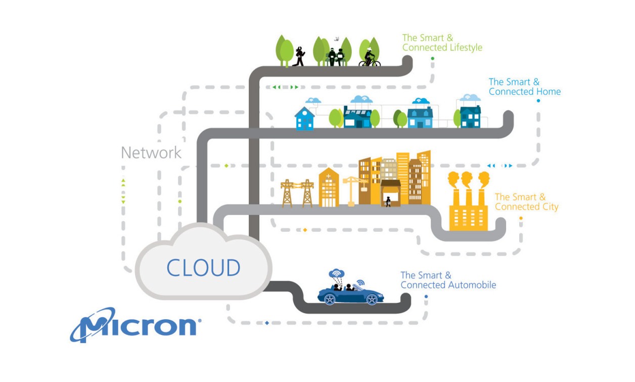
The Internet of Things (IoT) and its M2M products are bringing some of the most exciting advances in electronics to the forefront of our lives. Most new products and rich M2M services are being scaled for 3G technology. Designers have several options when selecting the right M2M memory solution – from industrial-grade NOR flash to NAND flash MCP solutions. Density, performance, size, P/E cycle, and data retention requirements are all important factors to consider.
References
[1] Mike Dano, “Sierra: 2G M2M sales for long-term apps in the U.S. are over,” FierceWireless, February 27, 2013
[2] “Mobile M2M Modules, Biannual Worldwide and Regional Market Size and Forecasts,” Infonetics Research, 1st Edition, May 31, 2013
Micron Technology • www.micron.com • @MicronTech • www.linkedin.com/company/micron-technology • www.youtube.com/user/MicronTechnology • www.micron.com/about/blogs