System in package designs provide big integration for SWaP-sensitive systems
February 08, 2017
System in packages (SiPs) promise to take integration to the next level –past the limits of lithography, in a sense – packing more performance and more battery life in a smaller form factors for...
System in packages (SiPs) promise to take integration to the next level –past the limits of lithography, in a sense – packing more performance and more battery life in a smaller form factors for wearables and a range of other size, weight, and power-sensitive (SWaP-sensitive) systems.
Wearable devices such as smart watches and fitness trackers suffer from a challenge that has long plagued embedded developers – balancing SWaP. Modern wearables incorporate not only a power-efficient processor with the ability to compute complex sensor fusion algorithms, but also the sensors themselves, Wi-Fi or Bluetooth Low Energy (BLE) to connect with a tethered mobile device or directly to the cloud, and often additional discrete memory ICs to support desired applications. All of this must be packaged within systems that provide the smallest possible charge time and form factors to meet the convenience and style demands of today’s consumer, while leaving the door open for advanced enabling technologies that can support next-generation features. Per Jag Bolaria, Principal Analyst for Embedded and Servers at The Linley Group, “This can be addressed by SIP technologies that place the two die on a package.”
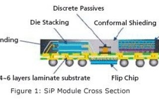
SiPs use a concept and architecture similar to a system on chip (SoC), integrating all the components of a system onto a single substrate. However, while an SoC requires homogeneous geometries, a SiP can integrate ICs with various geometries by stacking them in a single package. The result is a highly optimized, highly integrated solution that can fit easily into a confined space without sacrificing battery life or performance as you might find in conventional architectures based on discrete components, explains Yin Chang, Vice President of Sales at ASE Group.
“The idea of a SiP is to remove the lithography limit from the overall module,” Chang says. “We’re able to achieve a high-level of precision in putting down silicon and interconnects that can allow very close proximity between ICs,” says Chang.
“Connecting them through deposition traces, you can take advantage of maybe an analog 28 nm process and a very advanced 10 nm digital process on the processor side, and put it all together right next to each other and connect them through register-transfer level (RTL) solutions to build a large number of SiPs on a single process step,” he continues. “The device maker can mix and match.”
Custom and standardized SiP solutions help companies miniaturize their systems while enabling designers to add components and features without compromising size, performance, or battery life. According to Chang, this has lead to “more people seeing the benefits of putting components into SiPs.” For example, a wafer-level SiP solution can connect mobile silicon, allowing high density with a wide range of possible heterogeneous combinations including a single module that houses a processor with power management; a Wi-Fi or BLE connectivity chip; MEMS and sensors such as accelerometers, gyroscopes, magnetometers, and heartbeat sensors; as well as additional flash memory.
“The only thing you have to do is write firmware to connect the four pieces,” Chang says. “Leveraging an embedded silicon solution that puts silicon inside of a substrate and leaving all the paths on the outside tremendously reduces the X/Y footprint. I can take an individual SiP and mount it onto an embedded solution, put all the power requirements onto a wafer-level SiP, and then manage [energy efficiency] through a power IC that’s embedded in the substrate connected through a flex circuit. So you’re looking at more and more integration, but you are not limited by lithography.
“[This could apply to] a Wi-Fi module that’s in devices like augmented reality (AR) goggles and have a very small form factor, or a heartbeat monitor that can fit on your finger,” he adds.
Shortening time-to-market, increasing integration
Aside from the technical benefits, the goal of SiPs is to get solutions to market as quickly as possible. Many SiP manufacturers provide off-the-shelf solutions that are fully functional and tested, and offer testing and qualification services for custom designs and board-level integration. For SiP prototyping, ASE’s sister company Universal Scientific (USI) also provides integrated evaluation boards that have already been “SiPed” with pre-mounted Wi-Fi, BLE, and heartbeat sensor modules and outfitted with connectors for development purposes.
Meanwhile, Bolaria expects SiP technology to mature and “proliferate more broadly, providing another way to increase density without jumping a process node or using exotic materials that lack CMOS economies of scale.” Echoing these statements, Chang expects the advantages of tight integration with the technology to continue as smaller silicon geometries become harder and harder to attain.
“We want to take integration to the next level,” Chang says. “Now connections are not based on the PC board design limitations, but more silicon-like limitations. We can now manufacture SiPs on large panels that are routed by very fine geometries of tighter material – copper, gold, or whatever that might be – and that improves performance and allows them to run at higher frequencies.”