Argonne National Labs Uses AI to Accelerate, Optimize Semiconductor Fabrication Process
July 09, 2021
Story
The current global semiconductor chip shortage is causing a domino effect for global supply chains. Not only are the prices rising for newly manufactured cars, but all types of electronics, such as smartphones, laptops, and more.
As a means to slow down the shortage, researchers at Argonne National Laboratory, a U.S. Department of Energy national laboratory, have invented an AI-based solution that synthesizes semiconductor nano materials.
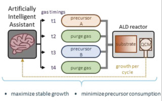
Most chip manufacturers utilize atomic layer deposition (ALD), a thin-film deposition technique for creating very fine films used to fabricate todays impossibly scaled-down microelectronics. The technique involves a gas-phase chemical process where the ALD reactions use two chemicals called precursors and reactants. The precursors react with the surface of each material one at a time, then a thin film is slowly deposited through repeated exposure to separate precursors.
ALD is an important process in fabricating semiconductor devices, but the downside is the lengthy trial-and-error process of making new films from each new material. For example, in order to identify optimal growth for each new material, materials scientists must arrange the complex chemistries between the molecular precursors; figure out when each dose of each precursor needs to be added; and determine the appropriate reactor design, temperature, and pressure.
Angel Yanguas-Gil, a Principal Materials Scientist at Argonne National Laboratory and co-author of a recent ALD research study, explains.
“Each cycle of growth and thickness characterization typically takes a few hours, with the exact duration being dependent of the process itself, variables such as the desired film thickness, and the availability of characterization tools,” he says.
“For challenging ALD thin film materials and precursors, it can take months to develop a working process.”
Automating ALD in Minutes with AI
Argonne researchers are the first to use AI to automate this process. They are using three approaches based on Bayesian optimization, random, and expert system algorithms to offer various ALD film combinations for the different materials.
The overall goal of these three approaches is to achieve the highest and most stable thin film growth in the shortest time using simulations that represent the ALD process inside a reactor. The Bayesian, random, and expert system techniques are tested by comparing how they affected the dosage and purge times of the two precursors used in ALD, where the dosage time is the time it takes to add the precursor to the reactor and the purge time is the time to remove excess precursor and gaseous chemical products.

Figure 1. Argonne National Laboratories researchers are using AI algorithms to create a closed-loop process that cuts ALD materials fabrication time by orders of magnitude.
Noah Paulson, a computational scientist at Argonne and the lead author comments, “In a closed-loop system, the simulation performs an experiment, gets the results, and feeds it to the AI tool. The AI tool then learns from it or interprets it in some way, and then suggests the next experiment. And this all happens without human input.”
The lack of human involvement cuts down on the time it takes to test each combination of materials.
"All of these algorithms provide a much faster way of converging to optimum combinations because you’re not spending time putting a sample in the reactor, taking it out, doing measurements, etc. as you typically would today,” says Yanguas-Gil. “Instead, you have a real-time loop that connects with the reactor.”
The expert system algorithm was developed fully in house at Argonne National Laboratories and the Bayesian approach was built using open-source tools like the scikit-learn Python library.
“The experimental demonstration has been done in our custom reactors at Argonne, which gave us the possibility to tinker with the software controlling the deposition tool,” Yanguas-Gil continues.
By utilizing all three AI techniques in their simulated system, Argonne researchers were able to measure film growth in real time after each cycle by forming a closed-loop system that automates algorithm optimization.
According to the researchers, the “in-situ techniques ... can reduce the turnaround to just a few minutes, so at least one order of magnitude [time] reduction.”
Making AI Accessible to the Semiconductor Manufacturing Industry
As previously stated, this was the first study to show how thin-film optimization can work in real time using AI. However, the benefits of the closed-loop process in optimizing and automating ALD could be applicable to certain organizations in the microelectronics industry moving forward.
“Our approach will be more valuable for those companies in need of establishing new processes,” Yanguas-Gil explains. “This includes companies supplying deposition tools to fabs, which have to constantly adapt and respond to their customers' needs.
“The advantage of our approach is that it can be adapted to work with commercially available and off-the-shelf hardware,” he says. “Anything that we've done is within reach of existing tool manufacturers.”
For more information on the research, read the study at: https://pubs.acs.org/doi/10.1021/acsami.1c00649
Tiera Oliver is the assistant managing editor at Embedded Computing Design. She is responsible for web content editing, product news, and story development. She also manages, edits, and develops content for ECD podcasts, including Embedded Insiders.
She utilizes her expertise in journalism and content management to oversee editorial content, coordinate with editors, and ensure high-quality output across web, print, and multimedia platforms. She manages diverse projects, assists in the production of digital magazines, and hosts company podcasts by conducting in-depth interviews with industry leaders to deliver engaging and insightful discussions.
Tiera attended Northern Arizona University, where she received her bachelor's in journalism and political science. She was also a news reporter for the student-led newspaper, The Lumberjack.