Hybrid Innovations for Processor Architecture Exploration
July 20, 2021
Story
Architecture exploration has been the holy grail of product design. It has the potential to completely transform product engineering. Research and use cases evaluations have shown that 80% of system optimization and almost 100% of the performance/power trade-offs can be achieved during architecture exploration.
Unfortunately, architecture exploration has failed to take off except in niche pockets where the company has invested significant resources and time. Architecture exploration has been highly misunderstood, and products have been introduced that claim architecture exploration but are wrappers around existing products such as Instruction Set Simulators, software timing analyzers, and hardware verification. Highlighting a language with a set of class libraries is insufficient to establish a methodology, easily create models, validate against benchmarks, and performance system optimization.
The major impediment to architecture exploration is the lack of architecture models for high-end cores, interconnects, cache, and memories. The limited range of models tend to be for low-end processors where architecture exploration does not add significant value, cycle-accurate models that run a maximum of 1,000’s of instructions per second, take a long time to install, learn, and assemble, and are released well after the IP has been shipped. These models take weeks to run one benchmark and are useful for comparative verification. Also, they do not scale across core, SoC, system, and software.
Architecture models tend to be a low priority for IP providers and EDA vendors, as they must deliver RTL and software tools such as compiler, debuggers, and verification IP. Also, creating architecture models for large-scale distribution requires a special skillset, as the process starts afresh for each core type. It takes a long time to assemble, requires multiple resources, and runs extremely slow. Each of the new processor cores have so many variations- read/write widths to caches, multi-threaded, ISA versions, variable pipeline stages, schedule logic for instruction dispatch to execution units, and instruction buffer.
Traditional architecture models with stochastic and is used by companies assembling large systems and data centers. The models would emulate the latency and power consumption for different types of requests and tasks.
Another major problem is the process of validation. For a new processor, there is limited benchmark data to verify the accuracy of a model. This problem is even more acute for the power, cache hit-miss ratio, and memory throughput. Of course, FPGA boards can take some of the load off by using an older version of the core with the updated settings of the cache, interconnect, and memory. The best way to test the correctness of new cores is to meticulously check every possible scenario including concurrent execution, run older traces for the cache hierarchy and DMA, and generate a scenario that ensures absolute coverage.

Figure 1: Architecture Exploration of Processors using VisualSim based on RISC-V and ARM
One approach that has been recently taken by Mirabilis Design is to deliver a Hybrid Processor Architecture Library on a Discrete-Event Simulator with a graphical development environment. This category of architecture models eliminates all the problems of the earlier approach. This is a common generator that uses a spreadsheet to define the core configurations. An internal sequencer optimizes simulation performance by eliminating logic that does not impact flow correctness, performance, and power, and provides a flexible list of options to define the different pipeline variants. The beauty of this approach is that new or even non-existent cores can be quickly constructed.
This approach has multiple benefits including:
- A single library block can model a micro-controller to a high-performance processor.
- The processor library has the simulation performance to investigate a single cluster, group of multi-core clusters, System-on-Chip, and a full system such as ECU, radar, or Supercomputers.
- This approach provides a large library of vendor cores.
- The Hybrid core diverges from the stochastic cores with the ability to run software traces.
- The extended library has all the connectivity and methods that make the generated cores to be fully integrated with caches, Dynamic System cache, TileLink, AMBA AXI, NoC, DDR, LPDDR, GDDR, DMA, and Bridges.
These models using the Hybrid Processor can be used to select the clock speed, buffer size, width, and capacity, while providing the topology, routing, flit size, and device connectivity. On the power side, the system model can determine the best set of power states and the optimal power management algorithms. Analyzing the power at this early stage provides insight on power distribution, battery capacity, charging systems, and thermal requirements. The accuracy of the Hybrid models enables the software performance tuning and selection of schedulers and arbiters.
The required metrics that need to be generated for performance are latency, throughput, buffer occupancy, hit-ratio, pipeline stall, MIPS, and cycles/instruction. To conduct a true power analysis metrics on the average and instant power, energy dissipated, power per task and device, and the impact of the energy management algorithms. Advanced analysis will cover the functional correctness, behavior in the event of failures, and the quality of service.
The attributes to be defined in the Hybrid Processor include the ISA assignment to execution units and latency cycles, number of floating point and integer units, cores per cluster, distribution of In-order and Out-of-Order, and number of large/small cores. The cache configuration can cover inclusion/exclusion, capacity, associativity, bank count, use of scratchpad, and various replacement and write policies. For the interconnects, the throughput requirements, buffer occupancy, the most efficient arbitration algorithms, and the transfer burst/flit sizes. At the memory, the model can measure bandwidth, latency and open/closed page for traces, sequential, and random addresses.
At the SoC-level, there is use of DMA vs TCP transfer, Tensor operation exploration and split-lock arrangements. The system must be tested for task partitioning across clusters, memory controller scheduling, number of routers, and device connectivity. As the system gets closer to customer deployment, the same models can be expanded to integrate multiple processor integration, minimize chip-to-chip overhead, distribution of applications to processors, and storage strategy.
Architects can select from the vendor list or create a new one in a few days. Once the processor core has been instantiated, the user can connect the other semiconductor IP to form the full SoC. In a short period of time, the user can have a multi-core multi-cluster, NoC-based SoC with GPUs, TPU/AI accelerators, memories, displays controllers, Ethernet, and other interfaces. To simulate this model, the IO are triggered with data streams generated with Poisson distribution and data ranges, and the processor executes software traces to execute simulation. Multiple SoCs can be combined via a coherent PCIe or CXL or connected with a high-speed Ethernet network or a reliable OpenVPX backplane.

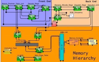
Figure 2: System-level model of an Out-of-Order processor pipeline with cache-memory hierarchy; Source: VisualSim Architect
The new Hybrid Processor is instruction-aware for load/store behavior, executes as in-order/out-of-order, supports multi-instruction fetch and dispatch, supports different attributes for each pipeline stage, supports flow control between stages, queues for task issue, jump pipeline stages, buffering between pipeline and cache, variable read and write width, and preemption support. The Hybrid approach can scale to 20 execution units of type integer, float, vector, branch, load, and store. At the same time, the number of pipeline stages can be variable per execution unit and can be defined up to 20.
All these new features for Hybrid Processor support the execution software traces with cache addresses. To prepare the software for executing on this processor model, a fully automated system generates the instruction sequence, instruction cache address, and data cache addresses for load store. The combination of the architecture model with the traffic and the software execution provides an efficient platform to test for accuracy of the core, caches, interconnects, and memories. The test covers both the latency and the power consumed for the end-to-end design, but also measures the cache hit-ratio and memory throughput. This new benchmarking approach instills confidence in the user and ensures for high quality trade-off analysis.
The new Hybrid Processor can be used by system companies developing custom SoCs using ARM or RISC-V cores, semiconductor companies integrating multiple non-heterogeneous masters, accelerators, GPUs and others processing units, and AI companies implementing new application and advanced AI/ML workloads. Competition for systems and semiconductors are significant in all markets and the time schedule to new products is shortening. Due to the semiconductor shortage, companies must use existing SoCs for longer duration, identify new applications, and support increased functionality on existing devices. Doing extensive architecture coverage will provide a detailed view into the realistic performance and capacity, thus providing valuable insight to customers that are integrating the product into their environment.

Figure 3: Multi cluster-Multi core Processor with Aaa65AE for automotive safety-critical applications; Model source: VisualSim Architect
An important side benefit of the Hybrid Processor is the ability to run the software and get an accurate view of the software performance on a target configuration. Today’s SoC configurations are so complex that running it on an FPGA will cause you to miss out the coherency, data allocation, workload distribution across clusters, and the intricate communication between the datapath and the caches. Software teams get early visibility into the timing and power consumption when the set of software tasks are running concurrently on the multi-core architecture.
Similarly, each core provides variations in the cache hierarchy organization and connection with items such as Write Back, width, block size, prefetch condition, banks, associativity, private vs. system, and so on. Then there are the memories from DDR, LPDDR, GDDR, HBM, and different types of schedulers in the commercial memory controllers. Finally, the different interconnect options: vendor-specific network-on-chip, extremely small NoC, AMBA variations, and Tilelink. To this add the DMA, bridges, interrupts, Dynamic Shared Cache Unit, IO, Ethernet, CAN/CAN-FD, and PCIe to get the complete requirement.
The Hybrid Processor is a major innovation in the electronic design industry. It provides more power in the hands of the Architect and enables the team to visualize the system behavior prior to development. As the speed of analysis is quick, true architecture coverage is possible and can cover performance, power, quality-of-service, efficiency, reliability, and functional correctness. With the addition of software performance analysis and tuning, all the system teams can engage within the same environment. Hybrid Processors are the future as designers engage with new applications, small process technologies, and increasing power requirements.
Deepak Shankar is the founder of Mirabilis Design, Mr.Shankar has over two decades of experience in management and marketing of system level design tools. Prior to establishing Mirabilis Design, he held the reins as Vice President, Business Development at MemCall, a fabless semiconductor company and SpinCircuit, a joint venture of industry leaders Hewlett Packard, Flextronics and Cadence. He started his career designing network simulators for the US Federal Agencies and managing discrete-event simulators for Cadence. His extensive experience in product design and marketing stems from his association with the EDA industry in multifaceted roles. An alumnus of University of California Berkeley with an MBA, he holds a MS in Electronics from Clemson University and a BS in Electronics and Communication from Coimbatore Institute of Technology, India.