Three ways to improve PCB design productivity and predictability with hierarchical interface-aware design capability
August 01, 2014
System designers are increasingly relying on standards-based interfaces to help them meet market demands for products that are faster, boast more band...
Faster performance, more bandwidth, and low power – it’s a familiar refrain that continues to influence PCB design. To meet these demands, system designers rely on standards-based, high-speed interfaces such as DDRx and PCI Express. Also driving increased use of these protocols are the requirements of today’s ARM core-based processors. Design engineers use these protocols to support plug-and-play compatibility between the processors and peripherals and other devices. This is driving a change in the way PCB designers author and plan their designs.
However, many design authoring tools still don’t make it any easier to author with standards-based interfaces. Design engineers need to author at the interface level and to visualize, design, and constrain interfaces hierarchically. But traditional tools have limitations because they involve working with busses or bundles, with a single-level hierarchical definition of a group of signals.
Fortunately, new technology is paving a more efficient path.
Hierarchical interface-aware design technology integrated into a PCB design flow can improve PCB design productivity and predictability in three ways:
· Faster design authoring
· Better component placement
· Better routing
Faster PCB design authoring
Today’s high-speed interfaces simply can’t be modeled in a single-level hierarchy, an approach that traditional PCB design tools support. Consider, as an example, a DDRx interface with eight byte lanes – that is already one level of hierarchy. Each byte lane would have data signals, strobe signals, and mask signals – a second level of hierarchy. And, each grouping of signals would have its own set of signals, such as data signals with eight bits in a byte; this is the third level of hierarchy. To the system designer, these hierarchical levels are a natural way to group the different signals. As such, a tool that supports multiple hierarchies makes it much easier for the designer to work at a higher level of abstraction, applying constraints to signals that are logically grouped and at the interface level. This process accelerates design authoring because the designer can connect at the interface level, rather than the pin or net level.
Better component placement
When it comes to interconnect place-and-route challenges around high-speed interfaces, designers must deal with increasing:
· Number of constraints
· Density
· Number of large pin count devices, along with shrinking pin pitches. This calls for breakout planning, rather than traditional fan-out.
· Time to route designs, amidst shrinking design cycle time and resources
An interface-aware design methodology allows the designer to finalize critical component placement, streamline route planning, and perform feasibility analysis. The capability supports creation of a graphical object in the schematic for instantiating interfaces and hierarchical net groups, configuring. and connecting interfaces to components and blocks.
The front-end designer can also create interfaces (hierarchical net groups) and, via a netlist, pass this information on to the layout designer. The interface-aware design capability supports creation of interface bundles that visually guide the designer through critical component placement, as well as planning for routing. In fact, layout decisions can happen earlier in the design cycle, ensuring that placement will be good for routing. What’s more, the designer can take advantage of interface definitions for signal integrity analysis, shortening the required set-up time.
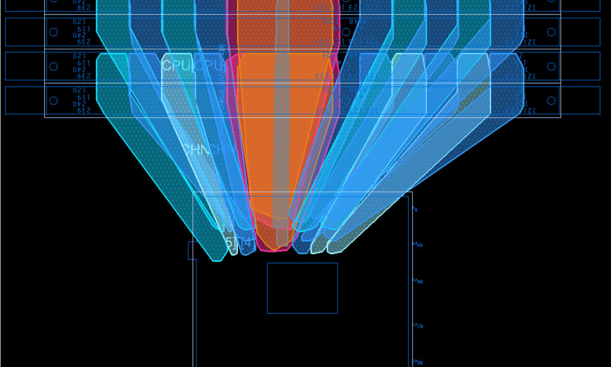
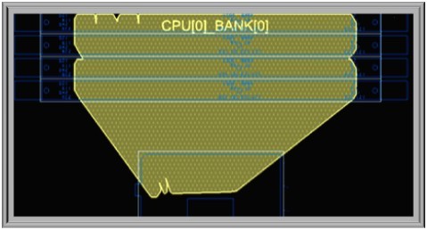
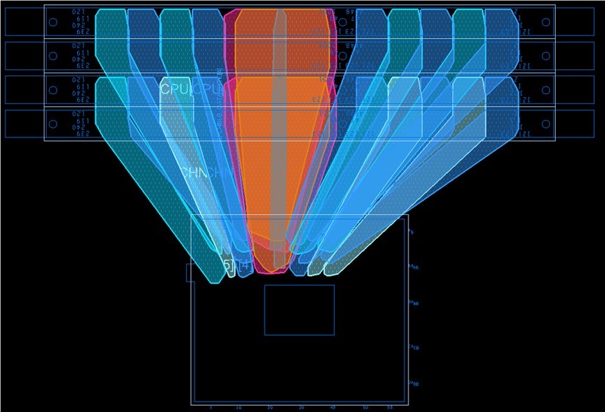
With traditional tools, component placement with all the to-be-connected lines on is difficult or can be confusing (Figure 1). By contrast, with interface-aware design, the engineering team starts off with a hierarchical block that represents the entire memory system and its connectivity to the processor. The visual representation of this diagram is a polygon (parts already placed) that shows a perimeter of all of the pins on the processor, the DIMMs, and, if applicable, the terminators that are part of the memory subsystem (Figure 2). This is a net group view; using color coding, the engineering team can show sub-blocks of the interface, even further breaking this down into separate channels and then down into individual byte lanes and so on (Figure 3). The color-coding function also helps the engineer make better choices about layer distribution earlier on, if the design canvas features overlapping polygons. Essentially, this approach makes it easy to visualize what each group of nets is.
|
|

|
|
|
|
Better routing
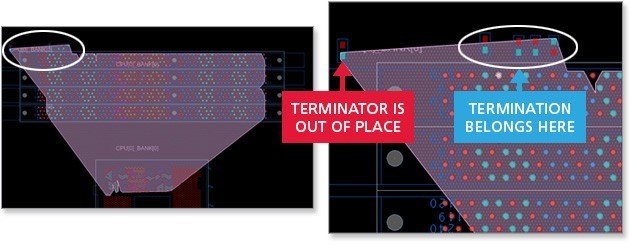
The interface-aware design capability also provides a way to visualize the overall routing domain of an interface, for fast and easy verification of the placements. Net groups are basically used as placement aids. The shape of the polygon on the design canvas encompasses the pins of the nets in a given net group. As the engineer places or moves components, the polygon changes its shape dynamically. Polygons with odd shapes are an indicator that there are improperly placed components. In Figure 4, for example, a terminator that is out of place creates an unusual angle because it is pushed off to the side.
|
|
Interface-aware design capability
Using a tool flow with hierarchical interface-aware design capability such as Cadence’s Allegro tool flow, engineers can achieve up to 15 percent faster design authoring and implementation. In addition, they can increase quality, performance, and reliability of PCB designs that utilize high-speed interfaces such as DDRx, PCI Express, and Serial ATA.
As part of the Allegro PCB design flow, engineers can also tap into auto-interactive technology to further accelerate breakout, routing, and tuning of interfaces. For example, auto-interactive breakout technology saves time in breakout and routing by helping to plan breakout of components tied to an interface and reducing routing steps. And, auto-interactive trunk routing routes the “trunk,” or main section of an interface, working with auto-interactive breakout tuning to flow the bundle.
Design help for high-speed interfaces
A PCB design flow with an integrated hierarchical interface-aware design capability helps designers working with high-speed interfaces accelerate design authoring, component placement, and route planning. It provides visual clues to let the designer know when there are component placement and routing issues. They can then resolve these issues before they get too far down the path of their design, when such problems are more costly to fix.
Cadence
www.cadence.com