28-nm ADCs enable next-generation electronic warfare receiver systems
July 05, 2018
Product
The high-speed ADC is a primary design consideration in all wideband EW receivers and largely determines system architecture and overall detect and observe capability.
The high-speed ADC is a primary design consideration in all wideband EW receivers and largely determines system architecture and overall detect and observe capability.
The ever-present need for higher bandwidth and lower size, weight, and power (SWaP) in electronic warfare (EW) receivers, specifically those for signal intelligence (SIGINT) applications, has EW system designers continually looking for new developments and improvements in high-speed analog-to-digital converter (ADC) technology. While 65-nm ADCs approach their inherent, process-related performance and bandwidth limitations, newer 28-nm RF ADCs surpass these boundaries and form a new foundation for next-generation wideband receiver systems. A 28-nm process node’s smaller transistor widths and lower parasitics enable faster sample rates, wider analog input bandwidth, and integrated digital functionality and new receiver architectures, all while reducing power consumption and overall size.
The high-speed ADC is one of the primary design considerations in all wideband EW receivers and largely determines system architecture and overall detect and observe capability. Many performance characteristics of the high-speed ADC, including sample rate, bandwidth, and resolution, determine how the rest of the receiver is designed—from the analog RF domain to the DSP requirements.
As EW system designers continue to develop the next-generation receivers, the need for higher ADC bandwidth and greater resolution remains the perpetual industry trend. Higher sample rates and bandwidth allow for more spectrum to be digitized at once, easing design challenges in the RF domain and reducing sweep times while greater bit depth leads to increased performance and fewer false alarms and detections. This insatiable need for higher sample rate and better resolution has led high-speed ADC vendors to move to increasingly smaller transistor lithographic nodes (currently 28 nm and 16 nm) that enable these requirements without increasing device power consumption.
The fundamental benefits of 28-nm ADCs are integral in enabling the next generation of wideband EW receivers and form a new foundation on which future systems will be built. The 28-nm transistors have reduced parasitic gate capacitance, enabling faster switching due to the lower energy needed to drive the switching. Because of this and the smaller physical transistor size, ADCs can pack in more transistors per square mm, leading to potentially greater digital processing capabilities.
Taking the inherently lower power consumption into consideration, the 28-nm ADCs offer performance and capability requirements previously considered impractical on the ≥65 nm process. The greater sample rates (several GSPS and above) are attractive to EW system designers, especially for SIGINT, electronic protect (EP), and electronic support (ES) applications. Just as important as ADC bandwidth is the resolution, which allows for greater SNR/SFDR and subsequent ability to detect, observe, and process a target signal. Undersampling beyond the first Nyquist is also possible as a result of higher analog input bandwidths.
Moving to a 28-nm process lets allows mixed-signal semiconductor vendors integrate increasing amounts of digital signal processing and functionality into their high-speed ADCs with no increase in (or even a reduction of) system SWaP. Digital features like integrated NCOs (numerically controlled oscillators) and DDCs (digital downconverters) push converter performance boundaries and allow for easing of system design challenges related to the higher converter data rates and high digital interface power consumption. Taking advantage of the 28-nm process and increasing the on-chip DSP capabilities can also offload much of the processing load and power consumption from the processor.
While the 28-nm ADC enables a larger piece of the RF spectrum to be captured and observed, the signal of interest might still be of relatively small bandwidth compared to the ADC Nyquist bandwidth. Additionally, the vast amounts of data throughput from GSPS ADCs can lead to challenges finding a suitable processor and physically interfacing it to the ADC. Many 28-nm converters currently on the market use the JESD204B interface standard at lane rates above 10 Gbits/s, which can introduce board layout and signal-integrity challenges associated with routing Gbit SERDES (serializer/deserializer) JESD lanes.
Fortunately, through integrated NCOs/DDCs and on-chip DSP, the ADC can convert the signal of interest down to a lower frequency or baseband, apply digital filtering, and decimate the digital data output rate so that more intensive processing can be performed on portions of the captured spectrum. Tunable NCOs let the DDC sweep across the digitized spectrum so that the entire spectrum can still be analyzed, but with the added benefits of processing gain and lower digital data output rates. Adding multiple NCOs and DDCs in parallel allows the user to preconfigure and quickly switch and fast hop between the DDCs, further reducing sweep times since NCO tuning is removed from the equation.
The integrated DDCs offer a power savings in the digital JESD204B interface. JESD SERDES running at such high rates can add a watt or more, so decimating the data rate down to lower speeds is beneficial. As high-speed ADCs continue to push to higher sample rates, bit depths, and bandwidth, integrating DDCs and ADCs becomes more attractive for wideband EW receivers since the enormous amount of digital data from the ADC can become difficult to process with a low SWaP processor. More information and some practical examples on DDCs are available in the two-part series by Jonathan Harris, What’s Up with Digital Downconverters.
Realizing new receiver architectures
Heterodyne receiver architectures are well understood and have been proven over time. Historically, many microwave receivers have been implemented with dual down-conversion architectures. With the ADCs available in previous generations, the large ratio of operating band frequencies to ADC input frequencies made image filtering impractical with one down-conversion receiver architecture. New ADCs increasing in both sample rate and analog input bandwidth now make high-performance wideband single down-conversion architectures practical and easily realizable.
In an example single down-conversion receiver architecture, thefront-end LNA is chosen for noise figure performance (Figure 1). If needed, a limiter is added in front of the LNA to increase the front end’s survive power capability. An operating band filter is next to attenuate any out-of-band interference. Next, additional gain and/or gain control can be added as needed. Prior to the mixer, a low-pass filter can reduce RF harmonics that add to mixing spurious output.

[Figure 1 | Example single down-conversion receiver architecture.]
The mixer is a critical building block and chosen to optimize performance in the frequency translation bands of interest. Another low-pass filter following the mixer filters upper sidebands prior to amplification. Additional IF gain is added as needed. The antialiasing filter is typically the final component prior to the ADC and rejects any frequencies that can fold in band through the sampling process. The ADC is next and, although it’s last in the chain, is typically the first component chosen while the rest of the receiver is built around the ADC.
Now let’s review some considerations for selecting frequency plan options. Frequency planning is the process of selecting a frequency translation approach that, when implemented with the components available, yields the lowest spurious performance with reasonable filter designs. As RF engineers enter this decision for the first time, the number of options and repercussions of a suboptimal frequency plan can make this a daunting task. Fortunately, modern advances in both CAD tools and the available components have made frequency planning more manageable.
In general, a higher IF frequency in the second or third ADC Nyquist zone is preferred from a spurious perspective. Here, we’ll outline the benefits by first showing a frequency plan translating a 10-GHz operating band to the first Nyquist of a 3-GHz ADC, then show the benefits when operating in the second Nyquist zone.
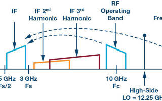
Figure 2 shows the frequency translation of a 1-GHz operating band at 10 GHz to the first Nyquist zone of a three-GSPS ADC. Two primary issues are illustrated. First, the RF image frequency is closely spaced to the operating band, requiring a difficult filter for image suppression. Second, any IF created from the IF amplification stages are in-band and unable to be filtered by the antialiasing filter.

[Figure 2 | Problematic frequency plan. The IF harmonics are within the IF band—this makes the image filtering difficult.]
Figure 3 shows a comparison when the same RF operating band is sampled in the second Nyquist zone. The higher IF frequency results in the image frequency that’s further from the operating band, and the RF image filters are easier to implement. In addition, any harmonics created in the IF amplifiers can be filtered by the antialiasing filter and the only IF harmonics that will be created are the ones inside the ADC itself.
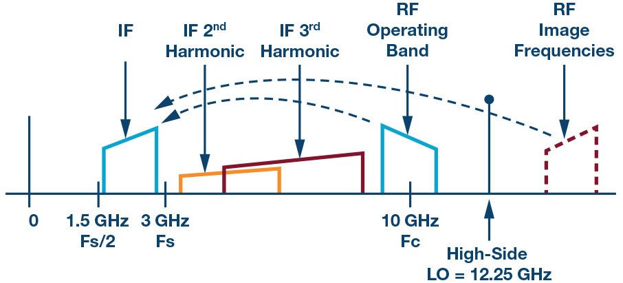
[Figure 3 | Improved frequency plan: The IF harmonics are outside the IF band, which means the image filtering is realizable.]
A spur analysis using the Keysight Genesys tool can be used to quickly come to the same conclusion. Figure 4, from the WhatIF frequency planning tool, shows that it’s set to a 10-GHz operating band, 1-GHz instantaneous bandwidth, high-side LO selection, and a search for up to fifth-order spurious. Spur free zones are shown in green and, in this case, fall in the second Nyquist zone of a three-GSPS ADC.
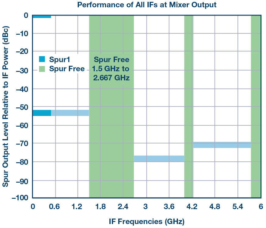
[Figure 4 | Spur analysis using the Keysight Genesys WhatIF frequency planning tool.]
Component enablers
As a follow up to any frequency plan analysis, mixers and ADCs should be evaluated under their intended operating conditions in the receiver to validate the spurious and noise performance. Recently released high performance 3- to 20-GHz mixers include the LTC5552 and LTC5553. The primary difference between them is that the LTC5552 has a differential IF output, while the LTC5553 is single ended on all ports. The differential IF output allows the entire IF chain to remain differential, thus eliminating the balun that’s normally added to the ADC input. Differential IF amplifiers are readily available by making a completely differential IF section realizable with the only design adjustment being the introduction of differential filters into the IF signal chains.
Another device, the 28-nm AD9208 ADC, is a 14-bit, three-GSPS, dual ADC with many of the feature sets and characteristics mentioned previously. The high input bandwidth and sampling resolution, along with digital features, like four integrated DDCs and NCOs, suit the AD9208 for many EW receiver systems and applications. Additionally, a 9-GHz analog input bandwidth lets the ADC directly sample up into the second and third Nyquist frequencies. Even fourth Nyquist sampling is possible with a clean, low-jitter reference clock to minimize SNR degradation at higher input frequencies.
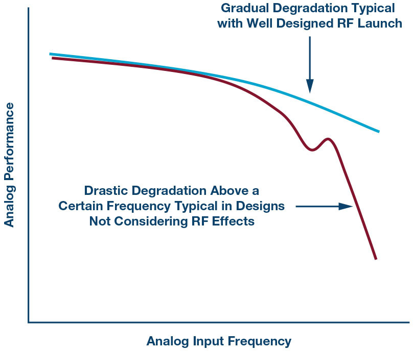
A continual challenge for the RF receiver designer is that every critical ADC metric degrades with input frequency. This is true for both noise and spurious-free dynamic range. In addition to silicon limitations, careful packaging design accommodating for the RF launch from the silicon to the packaging laminate and from the package to the PWB is required to maintain input bandwidths for GHz converters.
[Figure 5 | Analog performance: SNR, SFDR, and signal power all degrade with input frequency.]
Design for high IF sampling requires validating that the selected ADC doesn’t significantly degrade with the required input frequencies. In addition, careful RF layout techniques are required with the implementation in a PWB design. A well-designed RF I/O structure will have gradual degradation vs. input frequency. Without these considerations, there’s typically an input frequency where the performance drastically degrades (Figure 7). When screening converters for an application, much effort is spent validating performance prior to committing to a design. For RF sampling ADCs operating well into the GHz frequencies, this is more important and the performance response vs. frequency should be well understood prior to ADC selection for an application.