Low Noise and Low Power DAQ Solution for Seismology and Energy Exploration Applications
August 05, 2021
Story
Precision data acquisition (DAQ) systems are popular in industrial applications. In some DAQ applications, low power and ultralow noise are required. One example is seismic sensor-related applications, where a lot of information can be extracted from seismic data that is useful for a wide range of applications such as structural health monitoring, geophysical research, oil exploration, and even industrial and household safety (Reference 1.)
DAQ Signal Chain Requirements
Seismic geophones are electromechanical conversion devices that convert ground vibration signals into electrical signals. They are suitable for high resolution seismic exploration. They are implanted in the ground along arrays to measure the time of returns of seismic waves as they are reflected off discontinuity surfaces such as bedding planes, as shown in Figure 1.

Figure 1. Seismic source and geophone array.
To capture the small output signal from the geophones, a high sensitivity DAQ signal chain must be built for data analysis. The total rms noise should be = 1.0 µV rms with a limited flat low-pass bandwidth range of 300 Hz to ~400 Hz, while the signal chain should achieve a THD of around –120 dB. Since the seismic instrument is battery-supplied, the power dissipation should be balanced around 30 mW.
This article introduces two signal chain solutions to achieve the following targeted requirements:
- Gain of PGIA: 1, 2, 4, 8, 16
- ADC with integrated programmable wideband filter
- RTI noise at gain = 1 (300 Hz to ~400 Hz with –3 dB bandwidth) with 1.0 µV rms
- THD: –120 dB at gain = 1
- CMRR at gain = 1 with >100 dB
- Power consumption (PGIA plus ADC): 33 mW
- Secondary channel for self-test
Seismic Signal Chain – Example 1
There is no single precision ADC that has all these features and that can achieve such low noise and THD, nor is there a PGIA that can provide such low noise and low power. The challenge for developers is to determine the tradeoffs between using different components to build signal chains that achieve the target requirements.
For a seismic signal chain, a low noise, low distortion, and low power consumption PGIA is required. The ultralow noise ADA4084-2 or zero-drift amplifier ADA4522-2 are good candidates for such a configuration. Alternatively, the 24-bit sigma-delta ADC AD7768-1 or 32-bit SAR ADC LTC2500-32 are suitable for very high precision and provide configurable ODR with an integrated flat low-pass FIR filter for different DAQ applications.
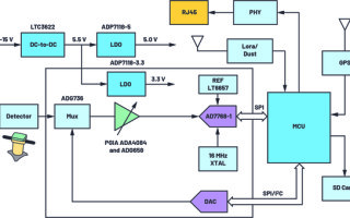
The total seismic signal chain is shown in Figure 2. In this example, the ADA4084-2, the ADG658, and 0.1% resistors can build a low noise and low THD PGIA for up to eight different selectable gain options. The AD7768-1 is a single-channel low power, –120 dB THD platform. It has a low ripple programmable FIR, DC to 110.8 kHz digital filter, and it uses the LT6657 as its reference device.

Figure 2. ADA4084-2 PGIA and AD7768-1 plus MCU filtering signal chain solution.
AD7768-1 can get 1.76 µV rms noise running at an ODR of 1 kSPS with power consumption of 10 mW in low power mode. To achieve a final 1.0 µV rms noise, it can run at higher ODR, such as 16 kSPS in median mode. When AD7768-1 runs at higher modulator frequency, it has a lower noise floor, as shown in Figure 3, with higher power consumption. A flat low-pass FIR filter algorithm can be implemented in the MCU software to remove the higher bandwidth noise and decimate the final ODR to 1 kSPS. The final rms noise will be around one fourth of 3.55 µV, which is 0.9 µV.

Figure 3. Balancing the AD7768-1’s ODR for targeted noise with MCU postfiltering.
As one example, the MCU software FIR filter can be made as shown in Figure 4 to balance performance and group delay.
Seismic Signal Chain – Example 2
The LTC2500-32 is a low noise, low power, high performance 32-bit SAR ADC with an integrated configurable digital filter. With 32-bit digitally filtered low noise and low INL output, it is targeted for seismology and energy exploration.
A high impedance source should be buffered to minimize settling time during acquisition and to optimize the switch cap input SAR ADC linearity. For best performance, a buffer amplifier should be used to drive the analog inputs of the LTC2500-32. A discrete PGIA circuit must be designed to drive LTC2500-32 for both low noise and low THD, which is introduced in the PGIA section.
PGIA Implementation
The key specifications of a PGIA circuit include:
- Power supply: 5 V minimum
- Since the AD7768-1 has 19.7 mW, the PGIA circuit should be <13.3 mW to meet the 33 mW power consumption target
- Noise: the noise at gain = 1 is 0.178 µV rms, about 1/10 of AD7768-1’s 1.78 µV rms
There are three types of PGIA topologies:
- An integrated PGIA
- A discrete PGIA with an integrated instrumentation amplifier
- A discrete PGIA with an operational amplifier
Table 1 lists ADI’s digital PGIAs. The LTC6915 has the lowest IQ. With 50 nV/√Hz noise density, the integrated noise within the 430 Hz BW is 1.036 µV rms, which exceeds the 0.178 µV rms target. Because of this, an integrated PGIA is not a good choice.
Table 2 lists several instrumentation amplifiers, including the 300 µA IQ AD8422. The integrated noise within 430 Hz BW is 1.645 µV rms, so it is not a good choice, either.

Figure 4. MCU post-FIR filter stages.

Figure 5. ADA4084-2 PGIA and LTC2500-32 signal chain solution.

Figure 6. LTC2500-32 flat pass-band filter noise for different downsampling factors.
Table 1. Digital PGIAs
|
Part Number |
Gain (min) (V/V) |
Gain (max) (V/V) |
IQ/Amp (max) (mA) |
VS Span (min) (V) |
VS Span (max) (V) |
Input Voltage Noise (typ) (nV/√Hz)
|
|
1 |
4096 |
1.6 |
2.7 |
11 |
50 |
|
|
28 |
1300 |
1.8 |
2.7 |
5.5 |
32 |
|
|
70 |
1280 |
2.7 |
5 |
5.5 |
32 |
|
|
1 |
10 |
4.5 |
10 |
30 |
18 |
|
|
1 |
8 |
4.5 |
10 |
34 |
18 |
Table 2. Instrumentation Amplifiers
Table 3. Low Noise, Low Power Operational Amplifiers
|
Device |
VOS (max) (µV) |
IBIAS (max) |
GBP (typ) (MHz) |
0.1 Hz to 10 Hz VNOISE (typ) (nV p-p) |
VNOISE Density (typ) (nV/√Hz) |
Current Noise Density (typ) (fA/√Hz) |
IQ/Amp (typ) (µA) |
VS Span (min) (V) |
VS Span (max) (V) |
|
5 |
150 pA |
2.7 |
117 |
5.8 |
800 |
830 |
4.5 |
55 |
|
|
100 |
250 nA |
15.9 |
100 |
3.9 |
550 |
625 |
3 |
30 |
Noise Simulation
LTspice can be used to simulate the noise performance of a discrete PGIA. The integral noise BW is 430 Hz. Table 4 shows the noise simulation result of two different PGIAs and the AD7768-1. The ADA4084 solution has better noise performance, especially at high gain.

Figure 7. Block diagram of a discrete PGIA.
Discrete PGIA by Operational Amplifiers
The article “Programmable Gain Instrumentation Amplifiers: Finding One that Works for You” discusses the various integrated PGIAs and supplies good guidelines for building a discrete PGIA when trying to meet a specific requirement (Reference 2). Figure 7 shows the block diagram of a discrete PGIA circuit.
ADG659/ADG658 can be chosen with low capacitance and 5 V power supply.
For op amps, IQ (<1 mA per channel) and noise (<6 nV/√Hz voltage noise density) are key specifications. The precision op amps ADA4522-2 and ADA4084-2 are good choices, with their features listed in Table 3.
For gain resistors, 1.2 kΩ/300 Ω/75 Ω/25 Ω resistors are chosen to achieve 1/4/16/64 gain. With greater resistance, noise may increase, and with lesser resistance, more power consumption is needed. If another gain configuration is needed, resistors must be carefully chosen to ensure the gain accuracy.
A differential input ADC plays the role of subtractor. The CMRR of the ADC is >100 dB, which can meet the system requirement.
Table 4. Noise Simulation Result
|
|
ADA4084 PGIA and AD7768-1 |
ADA4522 PGIA and AD7768-1 |
|
RTI Integrated Noise Within 430 Hz BW and Gain = 1 (µV rms) |
1.765 |
1.774 |
|
RTI Integrated Noise Within 430 Hz BW and Gain = 4 (µV rms) |
0.744 |
0.767 |
|
RTI Integrated Noise Within 430 Hz BW and Gain = 16 (µV rms) |
0.259 |
0.311 |
|
RTI Integrated Noise Within 430 Hz BW and Gain = 64 (µV rms) |
0.148 |
0.225 |
In-Loop Compensation Circuit to Drive LTC2500-32
The AD7768-1 has an integrated precharge amplifier to ease the driving requirement. For SAR ADCs, such as the LTC2500-32, high speed amplifiers are normally suggested for use as the driver. In this DAQ application, the bandwidth requirement is low. For driving LTC2500-32, an in-loop compensation circuit using the precision amplifier (ADA4084-2) is suggested. Figure 8 shows the in-loop compensation PGIA used to drive the LTC2500-32. The PGIA has the following features:
- R22/C14/R30/C5 and R27/C6/R31/C3 are key components to better stability for in-loop compensation circuitry.
- With ADG659, A1/A0 = 00, gain = 1, and the feedback path of the upper amplifier is amplifier out ➞ R22 ➞ R30 ➞ S1A ➞ DA ➞ R6 ➞ AMP —IN.
- With ADG659, A1/A0 = 11, gain = 64, and the feedback path of the upper amplifier is amplifier out ➞ R22 ➞ R8 ➞ R10 ➞ R12 ➞ S4A ➞ DA ➞ R6 ➞ AMP —IN.
The PGIA is connected to LTC2500-32EVB to verify the performance. Different passive component (R22/C14/R30/C5 and R27/C6/R31/C3) values are tried to reach better THD and noise performance at different gain (1/4/16/64). The final components values are: R22/R27 = 100 Ω, C14/C6 = 1 nF, R30/R31 = 1.2 kΩ, C3/C5 = 0.22 µF. The measured 3 dB BW at gain = 1 below PGIA is about 16 kHz.

Figure 8. A PGIA to drive the LTC2500-32.
Bench Evaluation Setup
To test the noise, THD, and CMRR performance, a discrete ADA4084-2 PGIA and AD7768-1 board were made as a total solution. This solution is compatible with the EVAL-AD7768-1 evaluation board, so it can interface with the control board SDP-H1. Thus, the EVAL-AD7768FMCZ software GUI can be used to gather and analyze data.
The ADA4084-2 PGIA and LTC2500-32 board is designed as an alternative total solution. The board interfaces to the SDP-H1 controller board, which is controlled by the LTC2500-32FMCZ software GUI.
In both boards, the PGIA’s gain is designed as 1/2/4/8/16, which is different from what’s shown in Figure 8. Table 5 shows the evaluation results for these two boards.

Figure 9. ADA4084-2 PGIA and AD7768-1 evaluation board solution.
Table 5. Signal Chain Solution Test Results
|
|
ADA4084-2 and AD7768-1 (Median Mode, FMOD = 4 MHz, ODR = 16 kSPS)+ |
ADA4084-2 and AD7768-1 (Median Mode, FMOD = 4 MHz, ODR = 16 kSPS)+ MCU FIR and DEC to ODR = 16 k/16 = 1 kSPS |
ADA4084-2 and LTC2500-32 ADC MCLK = 1 MHz |
|
RTI Noise at Gain = 1 (μV rms) |
3.718 |
0.868 |
0.82 |
|
RTI Noise at Gain = 2 (μV rms) |
1.996 |
0.464 |
0.42 |
|
RTI Noise at Gain = 4 (μV rms) |
1.217 |
0.286 |
0.3 |
|
RTI Noise at Gain = 8 (μV rms) |
0.909 |
0.208 |
0.24 |
|
RTI Noise at Gain = 16 (μV rms) |
0.808 |
0.186 |
0.19 |
|
THD at Gain = 1 (dB) |
—125 |
—125 |
—122 |
|
THD at Gain = 2 (dB) |
—125 |
—125 |
—119 |
|
THD at Gain = 4 (dB) |
—124 |
—124 |
—118 |
|
THD at Gain = 8 (dB) |
—120 |
—120 |
—117 |
|
THD at Gain = 16 (dB) |
—115 |
—115 |
—115 |
|
CMRR at Gain = 1 (dB) |
131 |
131 |
114 |
|
CMRR at Gain = 4 (dB) |
117 |
117 |
121 |
|
CMRR at Gain = 16 (dB) |
120 |
120 |
126 |
|
Pd Typical (mW) |
31.3 |
31.3 |
33.2 |

Figure 10. ADA4084-2 PGIA and LTC2500-32 board FFT for gain 1.
Conclusion
To design a very low noise and low power DAQ solution for seismology and energy exploration, a discrete PGIA can be designed with low noise and THD precision amplifiers to drive a high resolution precision ADC. This solution is flexible to balance the noise, THD, and ODR against its power consumption requirements.
- Benefits from LTC2500-32’s low noise performance, as well as the ADA4084-2 and LTC2500-32, show the best noise performance without an MCU’s further filtering processing.
- Both the ADA4522-2 and ADA4084-2 have good noise performance at PGIA gain = 1. The noise performance is about 0.8 µV rms.
- ADA4084-2 has better noise performance at high gain. At gain = 16, ADA4084-2 and LTC2500-32’s noise is 0.19 µV rms, which is better than the 0.25 µV rms of the ADA4522-2.
- For the AD7768-1, with MCU’s filtering, the ADA4084-2 and AD7768-1 solution shows noise performance similar to the ADA4084-2 and LTC2500-32 solution.
This article gives a solution to data acquisition that requires both low noise and low power with limited bandwidth. There are other DAQ applications that require different performance. If low power consumption is not a must, then the following operational amplifiers can be used to build the PGIA:
- Lowest noise: the LT1124 and LT1128 can be considered to have the best noise
- Lowest drift: the ADA4523, a new zero-drift amplifier, has better noise specifications than the ADA4522-2 and LTC2500-32.
- Lowest bias current: the ADA4625-1 is recommended if the sensor’s outputresistance is high.
- Higher BW: The ADA4807, LTC6226, and LTC6228 are good solutions when building high BW, low noise PGIAs in high BW DAQ applications.
In DAQ applications where noise and power are not important but a small PCB area and high integrity are required, ADI’s new integrated PGIAs, ADA4254 and LTC6373, are also good choices. ADA4254 is a zero-drift, high voltage, 1/16 to ~176 gain robust PGIA, and LTC6373 is a 25 pA IBIAS, 36 V, 0.25 to ~16 gain, low THD PGIA.
Table 6. Precision Op Amp Selection Table
|
Part Number |
VOS (max) (µV) |
IBIAS (max) |
GBP (typ) (MHz) |
0.1 Hz to 10 Hz VNOISE (typ) (nV p-p) |
VNOISE Density (typ) |
Current Noise Density (typ) |
IQ/Amp (typ) |
VS Span (min) (V) |
VS Span (max) (V) |
|
5 |
150 pA |
2.7 |
117 |
5.8 nV/√Hz |
800 fA/√Hz |
830 µA |
4.5 |
55 |
|
|
100 |
250 nA |
15.9 |
100 |
3.9 nV/√Hz |
550 fA/√Hz |
625 µA |
3 |
30 |
|
|
80 |
75 pA |
18 |
150 |
3.3 nV/√Hz |
4.5 fA/√Hz |
4 mA |
5 |
36 |
|
|
70 |
20 nA |
12.5 |
70 |
2.7 nV/√Hz |
300 fA/√Hz |
2.3 mA |
8 |
44 |
|
|
500 |
3 µA |
60 |
220 |
1.9 nV/√Hz |
430 fA/√Hz |
1.15 mA |
3 |
12.6 |
|
|
100 |
250 nA |
15.9 |
100 |
3.9 nV/√Hz |
550 fA/√Hz |
565 µA |
3 |
30 |
|
|
125 |
1.6 µA |
200 |
160 |
3.3 nV/√Hz |
700 fA/√Hz |
1 mA |
2.7 |
11 |
|
|
5 |
300 pA |
5 |
88 |
4.2 nV/√Hz |
1 pA/√Hz |
4.5 mA |
4.5 |
36 |
|
|
40 |
90 nA |
20 |
35 |
850 pV/√Hz |
1 pA/√Hz |
7.4 mA |
8 |
44 |
|
|
95 |
25 µA |
890 |
940 |
880 pV/√Hz |
3 pA/√Hz |
16 mA |
2.8 |
11.75 |
|
|
95 |
20 µA |
420 |
770 |
1 nV/√Hz |
2.4 pA/√Hz |
5.5 mA |
2.8 |
11.75 |
References
- Geophones. ScienceDirect.
- Jesse Santos, Angelo Nikko Catapang, and Erbe D. Reyta. “Understanding the Fundamentals of Earthquake Signal Sensing Networks.” Analog Dialogue, Vol. 53, No. 4, December 2019.
- Kristina Fortunado. “Programmable Gain Instrumentation Amplifiers: Finding One that Works for You.” Analog Dialogue, Vol. 52, No. 4, December 2018.
About the Authors
David Guo is a product applications engineer for ADI’s linear products. He started working in the China Central Application Center of ADI as an applications engineer in 2007, and transferred to the Precision Amplifier Group as an applications engineer in June, 2011. Since January, 2013, David has worked as an application engineer in ADI’s linear product department. He is responsible for technical support of products including precision amplifiers, instrumentation amplifiers, high speed amplifiers, current sense amplifiers, multipliers, references, and rms-DC products. David earned his bachelor’s and master’s degree in mechano-electronic engineering from Beijing institute of Technology. He can be reached at [email protected].
Steven Xie has worked as a product applications engineer with the China Design Center in ADI Beijing since March 2011. He provides technical support for SAR ADC products across China. Prior to that, he worked as a hardware designer in wireless communication base stations for four years. In 2007, Steven graduated from Beihang University with a master’s degree in communications and information systems. He can be reached at [email protected].

David Guo is a product applications engineer for ADI’s linear products. He started working in the China Central Application Center of ADI as an applications engineer in 2007, and transferred to the Precision Amplifier Group as an applications engineer in June, 2011. Since January, 2013, David has worked as an application engineer in ADI’s linear product department.
Steven Xie has worked as a product applications engineer with the China Design Center in ADI Beijing since March 2011. He provides technical support for SAR ADC products across China. Prior to that, he worked as a hardware designer in wireless communication base stations for four years. In 2007, Steven graduated from Beihang University with a master’s degree in communications and information systems. He can be reached at [email protected].