What Is a Control System and How To Design a Control Loop for a DC-to-DC Converter
April 18, 2022
Story
This article will introduce basic control theory and discuss how to analyze the stability and bandwidth of a DC-to-DC voltage control loop. It may help designers to deeply understand control loop, as well as calculate circuit parameters accurately and quickly instead of using trial and error when encountering control loop problems.
Introduction
Loop compensation is a key procedure when designing a DC-to-DC converter. If the load in an application has a high dynamic range, designers may find that the converter no longer works smoothly and the output voltage is no longer stable, resulting in stability or bandwidth problems. Understanding the loop compensation concept is beneficial for designers dealing with typical power management applications.
This article is divided into three sections. The first two sections discuss the control system theory, general buck DC-to-DC converter topology, and how to design a DC-to-DC control loop. In the third section, we use the MAX25206 in an example of how to apply control theory to evaluate and design a DC-to-DC control loop.
A Brief Introduction to Control System Theory
Control systems are everywhere. Air conditioners control the room temperature, drivers control the direction of their car, and steamers control the temperature when cooking dumplings, etc. Control refers to the operation of a device or a physical quantity of the production process to achieve a variable to maintain a constant, or move along a preset trajectory along a preset trajectory dynamic process. Usually, systems in nature are nonlinear, but microscopic processes can be viewed as linear systems. In the semiconductor field, we consider microelectronics as a linear system.
The system that can realize automatic control is a closed-loop system, and the opposite is an open-loop system. The characteristic of the open-loop system is that the output signal of the system does not affect the input signal. Just like in Figure 1 where

Figure 1. Open-loop system.
G(s) is the transfer function of the system in complex frequency domain

VI is the input signal and VO is the output signal in s-domain. The closed-loop system in Figure 2 has a feedback path from output to input. The input node of the system will be the difference between the input signal and the feedback signal.

Figure 2. Closed-loop system.
When the controller iterates until the input signal is equal to the feedback signal, the controller reaches a steady state. Using the mathematical approach, you get the following closed-loop system equations:

Then the simplified equation is as follows:

Its denominator phase (Equation 4) is equivalent to the open-loop transfer function (also called loop gain). Its gain amplitude provides the strength of the feedback and its bandwidth is the controllable bandwidth of the closed-loop system. Of course, their phase shifts will also be superimposed. It should be known that if the loop gain is greater than 0 dB and, simultaneously, the phase shift is 180°, the control loop will work in positive feedback and will form an oscillator. This is a key point of stability design.
The designer should make sure that the phase margin and gain margin are within a safe range or the whole system loop will start to self oscillate.
General Buck DC-to-DC Converter Topology
Next, we look at the topology and control loop of a buck DC-to-DC converter.

Figure 3. Buck DC-to-DC block.
Figure 3 shows a typical buck converter schematic that was simplified to a small AC signal circuit. It includes three stages: a buck modulator stage, an output LC filter stage, and a compensation network stage. Every stage has its own transfer function.
The three stages constitute the whole control loop. The comparator and the half bridge form the buck modulator. The comparator input signal comes from the oscillator and from the compensation network. The compensation network is implemented in the closed-loop feedback path. The AC small signal gain of the modulator is

where VPP is the peak-to-peak voltage of the oscillator’s triangle wave. VCC is the input power of half bridge. In control theory, the small signal gain is equivalent to the transfer function. As you can see, the modulator does not have a phase shift, only a gain of amplitude. The LC filter transfer function is

where L and C are inductance and capacitance. This is an ideal state. Generally, there are parasitic parameters in the circuit, like in Figure 4.

Figure 4. LC filter with parasitic parameters.
DCR is the DC equivalent resistance of an inductor L. ESR is the equivalent series resistance of an output capacitor. Thus, the LC filter transfer function is

Obviously, the ESR would generate a zero for a control loop. When the ESR is too large to ignore, the designer should consider the stability issues that may be caused by ESR. A compensation network is used for eliminating the parasitic effects and improving the loop response.

Figure 5. Type II compensation topology.
The buck DC-to-DC block shows us a Type II compensation network. This kind of compensation circuit will provide one zero and two poles.

There are also Type I and Type III compensation circuits.

Figure 6. Type I compensation topology.

Type I is just an integration node. It is a minimum phase system.

Figure 7. Type III compensation topology.
A Type III transfer function is similar to Type II.

As you can see, a Type III transfer function is more complicated. It has two zeros and three poles. In Figure 7, an operational amplifier (OPA) was used for error amplification. An operational transconductance amplifier (OTA) can also be used for error amplification in the loop.

Figure 8. Type II compensation topology with OTA.
Its transfer function is similar to an OPA topology. The output voltage error signal was amplified and transformed to a current signal first by OTA, and then transformed into a voltage control signal by the compensation network. In any type of topology or amplifier that is selected, the zeros and poles must be located at the appropriate frequency.
How to Design a DC-to-DC Control Loop?
Let’s look at the whole open-loop transfer function of a buck DC-to-DC converter with a Type II loop compensation.

The transfer function of the modulator and LC filter cannot be changed easily.
We can only modify the compensation network.
Let us use Type II topology as an example. The Type II transfer function has two poles and one zero, as follows.
Fz = 1/RzCz;
Fp1 = 0;
Fp2 = R1(Cz + Cp)/R1RzCpCz;
The poles and zero positions are determined by loop gain and loop phase shift. A positive pole will add –20 dB/dec slope for gain curve in the Bode plot and will add a –90° phase shift for the loop phase curve in the Bode plot. Conversely, a positive zero will add a 20 dB/dec slope for the gain curve and will add a 90° phase shift for the loop phase curve. We can see that for the Type II compensation loop, there are two poles and one zero, and an LC filter with parasitics also has 2 poles and 1 zero. The parasitic poles may force a slope at the loop gain crossover point (the point at which the open-loop plot crosses the axis; where the gain is 0 dB) up to -40 dB/dec or even more. That means the system’s phase shift will reach 180° (the phase margin will reach 0°) and cause self-oscillation. The designer should avoid this kind of risk. Empirically, we should make sure the loop gain crossover slope is –20 dB/dec. To solve this problem, designers can only modify the compensation network. Modifying Rz or Cz can change the position of the zero and modifying Cp can modify the subpole. Usually, parasitic poles and zeros are located in very high frequency, so we place Fp2 a bit farther than Fz to force parasitic poles and zeroes under 0 dB. Both Fz and Fp2 will be the important factors of
loop bandwidth.

Figure 9. Type II Bode figure.
By adjusting the position of the poles and zeros, the frequency response and the phase response of the loop are changed.
As a result, we can achieve a balance between loop bandwidth and stability margin.
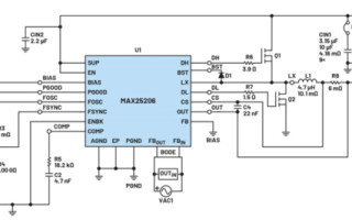
As an example, a schematic of the MAX25206 is shown in Figure 10. In the circuit, VOUT = 5 V, ILOAD = 3.5 A, so RLOAD = 1.43 Ω.

Figure 10. MAX25206 typical schematic.
Its compensation network is a Type II network with Cp = 0 pF (according to Equation 8). The second pole is located at infinity frequency and we can calculate the first zero from R5 and C2 at Fz = 1/(4.7 nF × 18.2 kΩ) = 11.69 kHz. In the output LC filter, we can get the zero from ESR and output capacitor by transfer function equation 7 at Fz = 16.4 MHz and the complex poles at Fp1 = 1.8 kHz –37.6 kHz and Fp2 = 1.8 kHz + 37.6 kHz. Predictably, Gf gain will reach the biggest point at 1.8 kHz. Gf gain will decrease rapidly when the frequency is larger than 1.8 kHz. Compensation zero Fz is a compensate for loop gain decrease. Also, we should know that the LC filter would resonate at 37.6 kHz if the loop gain is larger than 0 dB. Designers should not place Fz too close to 1.8 kHz to make sure that the loop gain does not go higher than 0 dB at 37.6 kHz. The AC loop simulated results are shown in Figure 11.

Figure 11. MAX25206 AC loop simulate.
Also, Type III can provide more potential for loop bandwidth and stability. Of course, to evaluate a system we should not only use the open-loop transfer function and the Bode plot, but we should also observe if the root locus of the closed-loop transfer function is in the left half plane and analyze the differential equation in the time domain. But in terms of convenience, observing the open-loop transfer function of the Bode plot is the most common and simplest method to achieve a stable power supply system design. The compensation loops, compensation methods, and theories are the same for other types of DC-to-DC topologies.
The only difference is the modulator, which is just the gain of the loop transfer function.
Examples of Other Compensation Network Topologies
In addition to different types of DC-to-DC topologies, there are also control loops with different schemes. Like the DC-to-DC converter, the MAX20090 LED controller is comprised of a current control loop. The converter senses the output current and feeds it back in to the control loop to reach the expected value. Another example is the MAX25206 buck controller with the function of limiting peak or average current. It senses both output voltage and average current and feeds them back. It is a double closed-loop controller. Usually, the current control loop is in the inner loop and the voltage control loop is in the outer loop. The bandwidth of the current loop (that is, the response speed) is greater than that of the voltage loop so it can achieve current limiting. The third example is the MAX1978 temperature controller. It contains an H-bridge that drives a thermoelectric cooler (TEC). The direction of different currents will determine the TEC’s heating or cooling mode. The feedback signal is the temperature of the TEC. Such a control loop will force the temperature of the output TEC to reach the expected temperature.
Conclusion
No matter what form of circuit topology, the basis of analog circuits for automatic control purposes is the theory discussed in this article. The designer’s goal is to achieve higher bandwidth and more robust stability, while balancing loop bandwidth and stability.
Yaxian Li is an applications engineer in the Training & Technical Services Group at Analog Devices. Yaxian joined Maxim Integrated in 2020 (now part of ADI) after graduating from Hangzhou Dianzi University with a bachelor’s degree in electrical engineering and automation in 2018. He can be reached at [email protected].