Applied Materials Introduces New Materials to Advance DRAM Technology
May 10, 2021
Blog
Memory technology doesn’t always advance at the swiftest pace, but there’s been some movement in this space as of late.
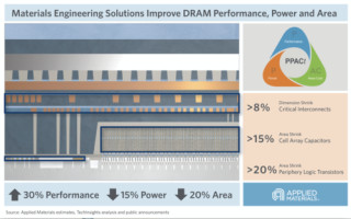
One example comes from Applied Materials, who announced a series of materials and engineering solutions designed to offer three new ways to scale DRAM products, while potentially accelerating improvements in chip performance, power, area, cost, and time to market. The target areas for these new products are in IoT and AI. This comes as “the industry urgently needs breakthroughs that can allow DRAM to scale and reduce area and cost while also operating at higher speeds and using less power,” according to Applied Materials.
The company is working with DRAM customers to commercialize three engineering solutions that create new ways to shrink as well as improve performance and power. The solutions target three areas of DRAM chips: storage capacitors, interconnect wiring, and logic transistors. All three technologies are now ramping into high volume production.
Because more than 55% of a DRAM chip’s die area is occupied by the memory arrays, increasing the density of these cells can have the largest impact on reducing the cost per bit. Data is stored as a charge in cylindrical, vertically arranged capacitors that need as much surface area as possible to hold an adequate number of electrons. As the capacitors narrow, they elongate for a maximum surface area. Applied Materials’ solution, dubbed Draco, provides a new hard mask material that’s optimized to work with the company’s Sym3 Y Etch system. The system is designed to increase etch selectivity by more than 30%, enabling a shorter mask.
A second strategy being deployed by Applied Materials is reducing the die area needed by the interconnect wiring that routes signals to and from the memory arrays. Each of the metal lines is surrounded by an insulating dielectric material to prevent interference between the data signals. Per the company, this eliminates the problem of thinning dielectric layers. The Black Diamond solution uses a low-k dielectric material that enables smaller, more compact interconnect wires that can move signals through the chips at multi-gigahertz speeds, without interference, and at lower power consumption.
The third advancement from Applied Materials is to improve the performance, power, area and cost of the transistors used in the chip’s periphery logic to help drive the I/O operations needed in high-performance DRAM. Previously, DRAM used transistors based on polysilicon-oxide that wasted power and limited performance. Today’s devices use a metal gate and a dielectric with hafnium oxide, a material that improves gate capacitance, leakage, and performance. That material is known as High-k metal gate, or HKMG.

Rich Nass is a regular contributor to Embedded Computing Design. He has appeared on more than 500 episodes of the popular Embedded Executive podcast series, and is a regular contributor to the Embedded Insiders podcast.
Rich has been in the engineering OEM industry for more than 35 years, and is a recognized expert in the areas of embedded computing, Edge AI, industrial computing, the IoT, and cyber-resiliency and safety and security issues. He writes and speaks regularly on these topics and more.
Rich is currently the Liaison to Industry for the Embedded World North America Exhibition and Conference, and has held similar positions with the global Embedded World Conference and Exhibition.
Previously, Rich was the Brand Director for UBM’s award-winning Design News property. Prior to that, he led the content team for UBM Canon’s Medical Devices Group, as well all custom properties and events. In prior stints, he led the Content Team at EE Times, handling the Embedded and Custom groups and the TechOnline DesignLine network of design engineering web sites.
Nass holds a BSEE degree from the New Jersey Institute of Technology.
Podcast/Interview Coverage
IEEE Awards Frede Blaabjerg Talks EVS
Atmosic: Embedded Executive: Energy Harvesting Podcast
Article Coverage
Embedded AI Isn’t Enterprise AI, and That’s a Good Thing
Tear Down: Google Pixel Watch 4
Protect Your Home from Thieves and Floods
Advantech Teams With AMD To Maximize Performance at the Edge
View additional information