Different Priorities
November 16, 2020
Whitepaper
When comparing 2D- and 3D-NAND, it is noticeable that the active area of the cell and the size of the memory area have increased significantly.
Flash memories that are suitable for industrial applications form a market of their own. While consumer or enterprise SSDs are built into well-ventilated systems, the suppliers of which cope well with the extremely short product lifetimes of storage media; industrial applications demand higher requirements. These include a much wider operating temperature spectrum and tolerance to the tougher environmental conditions in which boot and storage media in industrial machines or systems must perform their duties. Industrial storage media must also be offered unchanged for much longer in order to adapt to the extended lifecycles of equipment and devices in the industrial sector.
The fact that SLC-NAND features smaller data capacities compared to MLC and TLC and offers long-term module availability for fixed Bills of Materials, highlights just how different the priorities are for industrial flash memory. So, what is the situation with 3D-NAND? The innovation of 3D-NAND can be seen as an invigorating moment for the industry. For a long time, further miniaturization of memory cards and SSD seemed impossible. With 10 nm structure widths, a technological limit had been reached that was difficult to overcome in cost-benefit considerations. Only 3D-NAND opened the way for further miniaturization. In just a few years, increased vertical stacking of layers from 32 to 48 and 64 to 96 layers was achieved – and the development continues today. But does the technology also represent progress for industrial applications?
Actually, less prone to failure
When comparing 2D- and 3D-NAND, it is noticeable that the active area of the cell and the size of the memory area have increased significantly. The cell now bulges around the bit line and can accumulate much more charge. This makes storing bits as charge differences more reliable. The electrical interference from the neighboring cells could be reduced and therefore the signal-to-noise ratio improved.
However, these technological advantages were primarily used to expand storage capacity. That meant that storage space would become cheaper. At the same time, 3D-NAND offers the ability to increase the lifetime of the memory. For comparison: With 2D-MLC-NAND technology, each cell can be erased and reprogrammed 3,000 times. After this, the cell is degraded to such an extent that a minimum storage capacity of one year can no longer be guaranteed. With 3D-MLC-NAND, significantly more erase cycles would be technologically achievable. However, 3D-TLC-NAND is the predominant technology in the market. Here, the gain in charge in the cell was deployed to increase the number of bits per cell. As a result, the maximum number of erase cycles with 3D-MLC-NAND remains at 3,000 – and this, by the way, at great expense. While the 3,000 erase cycles from 2D-NAND could be achieved with a simple 40-bit per 1 KiB-BCH correction, at least 120-bit error correction is needed for the same 3,000 erase cycles with 3D-NAND. This new method, called LDPC, requires many more check bits and thus more silicon area in the controller, as well as more computing time for the correction software. This is especially true if the number of faulty bits increases at the end of the product’s life. Older controllers do not have the required resources and therefore cannot control 3D-NAND.
Greater firmware effort
Not only is error correction more complex with 3D-NAND, it also exposes new failure mechanisms that were previously unknown. This must be countered by new firmware functions. In particular, Block RAID should be mentioned here. With this feature, failures of a complete block can be corrected. This wasn’t possible before, but it wasn’t necessary either. Without this feature, system failures in the range of up to 1,000 DPPM (Defective Parts Per Million: failures per million devices) may occur. For consumer products this is still acceptable, and as such, Block RAID is usually not implemented. However, for industrial products such a failure rate is not acceptable. This makes the correction of block failures mandatory and requires both more complex firmware and the provision of greater redundancy. This occupies additional memory areas and increases the write gain (WAF), which in turn reduces the lifespan of the SSD.
Balance temperature sensitivity
There is another difference between 2D and 3D that increases the effort required: the cross-temperature effect. This is about the homogeneity of the cells in an array. With 2D-NAND, one could assume that cells in a page have the same capacity. 3D-NAND offers much better cell properties but exhibits very high scattering in its capacities. Here’s the reason: a bit line in 3D-NAND can be imagined as a thin hole etched through 64 layers. In the ideal case, a hole in the top layer would be just as large as one at the bottom of the stack. But the reality is different. The top layer has a much larger hole diameter than the bottom layer and therefore a completely different cell capacity and reference charge.
All 64 cells between the top and bottom layer belong to the same bit line and the same voltage detector. Within this bit line, the voltage levels vary widely and must be compensated for permanently. If changing temperatures are added, the work of the detector becomes very arduous indeed. For example, if you write at low temperatures and read at high temperatures, the voltage conditions are completely different than if you write at high temperatures and read at low temperatures.
All extreme temperatures are critical for 3D-NAND. Operating below -10°C or at +85°C causes reading problems by shifting the voltage levels. If further disturbances are introduced, data loss is imminent. For standard consumer 3D-NAND, the permitted change between write and read temperature is approximately 45 to 50 Kelvin. This means that one can write at 20°C and read at 65°C. For consumer products this is sufficient, but industrial temperature requirements are specified at -40°C to +85°C, for example. That would be a cross temperature of 125 Kelvin: two-and-a-half times higher than that permitted for consumer drives. Here too, 3D-NAND flash products that are specially optimized to meet industrial requirements are therefore required.
So just SLC after all?
Although 3D-NAND is more reliable than 2D-NAND at the individual cell level, the motivation to offer more memory at lower and lower prices has led to a steady decline in endurance and retention since the introduction of new technologies. As the above-mentioned characteristics of 3D-NAND have shown, extra effort must be made to ensure industrial usability. If applications require a service life in the range of 50,000 cycles or more due to high write volumes, SLC is still needed – especially if the write processes consist of small data blocks. However, the price gap continues to widen. SLC can now only be used where the technical requirements and the costs of replacing the memory are so high that the total product costs over its lifetime are lowest with SLC.
Interesting alternative: pSLC from 3D-NAND
There is an interesting trick being deployed in the field of industrial flash memory solutions to increase lifetime: Pseudo Single Level Cell (pSLC). SLC is more robust because only one bit per cell is stored and therefore the signal-to-noise ratio is higher. pSLC is an operating mode in which only two levels are used by a multi-bit cell (multi in this case being 2, 3, 4, etc.), i.e. the so-called MSB (Most Significant Bit). This increases the signal-to-noise ratio in the cell and reduces stress. So the cell can be deleted and reprogrammed more often. In practice, the number of erase cycles for MLC (2D) increases from 3,000 to 20,000 cycles when working with only one bit. This means seven times the endurance at just twice the price for the same capacity (as you only have half the number of memory bits available).
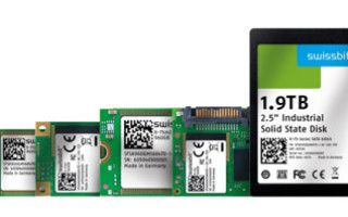
Swissbit also uses the pSLC mode for 3D-MLC or 3D-TLC. Due to the better cell characteristics, the gains are even greater here. Instead of 20,000 cycles with 2D-pSLC, 3D-pSLC now guarantees 30,000 to 40,000 cycles. The shelf life is still one year at the end of the lifetime. The company also offers a "Single Bit per Cell" variant with all new 3D-NAND products. Here, the term 3D-SLC is often used in a shortened form, as pure 3D-SLC does not (yet) exist. Due to the high over-provisioning and the high erase rate, a product in 3D-SLC mode is an ideal replacement for 2D-SLC and 2D-pSLC products with almost the same properties but at a significantly lower price. For example, the N-16m2 and N-18m2 are two PCIe/NVME M.2 SSDs; the X-76 family offers several form factors of SATA Gen3 SSDs (2.5", mSATA, M.2, SlimSATA); and the U-58 is a USB module with 3D-SLC technology. All impress with high performance and excellent durability.
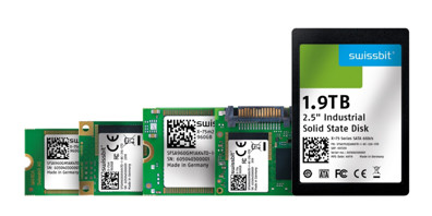
(Suitable for an industrial temperature range of -40 to +85°C: The Swissbit-X-75-SATA 6Gb/s SSDs, available as 2.5-inch SSD and in M.2 2280 and 2242 variants as well as mSATA and SlimSATA. (Image source: Swissbit))
3D-NAND for industrial storage
Of course, Swissbit uses a special NAND flash for its 3D products, which also supports the industrial temperature range and promises a very long product life. Together with the high-quality production and strictest QA standards, extremely robust storage media leave the factory in Berlin, Germany. But as the explanations have shown, the way the memory cells are used by the controller and firmware is also critical to their suitability in the respective application. With additional features like DRAM support, background refresh and thermal management, Swissbit 3D-SLC memory products offer fast, reliable and durable solutions at attractive prices. Industrial memory solutions are still possible even beyond the proven 2D-SLC chips. The bottom line is that the progress of 3D-NAND technology can be used to deliver endurance and retention – and not just for short-lived capacity gains.
About the Authors
Author:
Roger Griesemer, General Manager Memory Solutions at Swissbit AG, Bronschhofen/Switzerland
Co-author:
Ulrich Brandt, Director Technical Marketing at Swissbit AG, Bronschhofen/Switzerland