Functional safety, AI collide in automotive behind heterogeneous MIPS core
June 14, 2017
Blog
When I think of functional safety in the context of processing, I usually think of a small microcontroller (MCU) responsible for one or two dedicated tasks. Its architecture is probably simple...
When I think of functional safety in the context of processing, I usually think of a small microcontroller (MCU) responsible for one or two dedicated tasks. Its architecture is probably simple yet resilient in order to reduce the possibility of hardware faults and soft errors. This has been the case for safety-critical industrial and automotive applications for some time.
But, as the possibility of artificial intelligence (AI) technology creeping into many functional safety applications becomes a reality, simple MCUs become a less viable option. This is particularly true in the automotive industry, where AI is now a key component of many modern advanced driver assistance systems (ADAS) and emerging autonomous drive platforms. Camera-based machine vision, radar detection, driver condition evaluation, and multi-sensor fusion are all applications that stand to benefit from AI, but also demand much more processing power than an MCU can provide.
Thus, a gap is emerging in the market for higher performance processors capable of meeting the functional safety requirements of industry standards.
High-performance processor IP and ISO 26262 functional safety
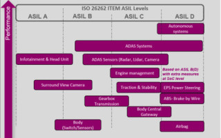
The design of any functional safety system begins at the processor IP level, and in the automotive industry the standard that governs such designs is ISO 26262. ISO 26262 comprises four Automotive Safety Integrity Levels (ASILs), ASIL A through D, with each addressing increasingly critical automotive systems (Figure 1). Some of the requirements for ISO 26262 compliance include:
- Evidence of safety processes and work products (ASIL B to D)
- Traceability of work products
- Technical safety assessment
- QA process compliance audit

[Figure 1 | The ISO 26262 standard outlines four Automotive Safety Integrity Levels (ASILs), A through D, for functional safety in hardware and software.]
The wrinkle in all of this for processor IP is that it is the responsibility of automakers and Tier 1 suppliers to ensure compliance with ISO 26262. IP blocks are part of a processor that is designed into a larger system, and it is in the best interest of IP vendors to design their solutions to suit many different applications.
One step IP vendors can take though is to ensure that their designs follow processes and procedures required for later ISO 26262 ASIL compliance. Known as a Safety Element out of Context (SEooC), this is the case with Imagination Technologies’ new 64-bit MIPS I6500-F CPU core.
On a technical level, MIPS I6500-F core includes several features that facilitate ISO 26262 compliance for automakers and Tier 1 manufacturers (Figure 2). These include support for:
- Runtime Logic Built-In Self-Tests (LBISTs) for hard and soft fault monitoring
- Time-out for fault recovery
- Bus parity for error detection during data transfer
- Error-correcting code (ECC) cache memories
- Redundant logic

[Figure 2 | The MIPS I6500-F CPU cluster includes several design features that help automotive manufacturers meet ISO 26262, as well as safety layers that isolate the core cluster, clocking and power blocks, memories, and I/O.]
These result of these design attributes are single-point fault metrics (SPFms) of better than 90 percent and latent fault metrics (LFMs) of better than 60 percent, enough to satisfy ISO 26262 ASIL B requirements and be extended to ASIL D.
Further, the I6500-F CPU cluster safety cycle follows the “V” model used by automotive manufacturers, helping match safety documentation from Imagination’s quality management system (QMS) flow to the documentation required for ISO 26262 certification (Figure 3). The core was designed using a mix of functional safety management processes and development practices, and verified by third-party safety assessor ResilTech.

[Figure 3 | The Imagination Technologies MIPS I6500-F CPU cluster matches the development cycle of an SoC used by automakers and Tier 1 manufacturers, while also allowing them to accelerate ISO 26262 ASIL D compliance with provided safety documentation safety documentation.]
Driving functional safety into heterogeneous automotive AI
As for performance, the I6500-F CPU is a heterogeneous multicore processor core capable of scaling to six cores per cluster and 64 clusters per SoC. Based on release 6 of the MIPS architecture, the I6500-F implements simultaneous multi-threading that allows each core to execute two instructions in parallel and up to four threads total (Figure 4). It targets 7 nm FinFET process technology.

[Figure 4 | The heterogeneous MIPS I6500-F CPU core enables highly scalable many-core SoC designs capable of leveraging simultaneous multi-threading on individual cores.]
The heterogeneous architecture of the I6500-F lends itself well to the design of AI systems that often implement additional accelerators like digital signal processors (DSPs) to run convolutional or deep neural networks (CNNs/DNNs). An AXI Coherency Extensions-compliant (ACE-compliant) interface provides communications directly with the control registers of these external processing elements in an SoC, as well as direct access to the I6500-F system bus for data traveling in the other direction. This is important in the framework of simultaneous multi-threading capability, as a single thread can be dedicated to managing an external accelerator without incurring the overhead of context switching.
Also key to efficient task transfer in such heterogeneous systems is a system-level shared virtual memory (SVM). SVM permits data to be passed through pointers rather than file copying, and contributes to system-level cache coherency during high-bandwidth AI data transfers (Figure 5). An ancillary benefit here is simplified software development, as critical safety and security tasks can be isolated from other applications using virtualization and a dual-level memory management unit (MMU).

[Figure 5 | A low-latency ACE interface and shared virtual memory (SVM) pair with the I6500-F core’s simultaneous multi-threading features to facilitate heterogeneous AI system architectures.]
Down the street from fully autonomous drive
The MIPS I6500-F could be an inflection point for artificially intelligent systems in that its pedigree in acknowledged industry safety standards provides a “known” backdrop against the “unknowns” of machine learning. Mobileye, for example, has designed the I6500-F into its next-generation EyeQ 5 SoC that will target fully autonomous driving applications by 2020.
The MIPS I6500-F CPU core is available for licensing now. SoC designers and automotive developers interested in learning how to integrate the core into their ISO 26262-compliant systems can contact [email protected] for information on design interface agreements (DIAs).