Is It Possible to Fit Low EMI Power Supplies onto Crowded Boards?
October 12, 2020
Story
Power supplies produce it, and it must be addressed, but what are the sources and what are typical mitigation strategies?
Limited and shrinking board real estate, tight design cycles, and stringent electromagnetic interference (EMI) specifications, such as CISPR 32 and CISPR 25, are limitations that make it difficult to produce power supplies that feature high efficiency and good thermal performance. Matters are further complicated by design cycles that often push power supply design to near the end of the design process—a recipe for frustration, as designers try to squeeze complex power supplies into tighter spots. Performance is compromised to finish designs on time, kicking the can down the road into test and validation. Simplicity, performance, and solution volume are traditionally at odds: prioritize one or two desired features and live with not having the third—especially when design deadlines loom. Sacrifices are accepted as normal; they should not be.
This article begins with an overview of a significant issue posed by power supplies in complex electronic systems: EMI, often simply called noise. Power supplies produce it, and it must be addressed, but what are the sources and what are typical mitigation strategies? This article addresses EMI reduction strategies, presenting a solution to reduce EMI, maintain efficiency, and fit power supplies into limited solution volumes.
What Is EMI?
Electromagnetic interference is an electromagnetic signal that disrupts the performance of the system. This disturbance affects circuitry by electromagnetic induction, electrostatic coupling, or conduction. It is a critical design challenge for automotive, medical, and test and measurement equipment manufacturers. Many of the limitations mentioned above and the increasing performance demands on power supplies—increasing power density, higher switching frequencies, and higher current—only serve to expand the effects of EMI, calling for solutions to reduce it. In many industries, EMI standards must be met, significantly impacting time to market if not considered early in the design cycle.
Types of EMI Coupling
EMI is a problem in electronics systems when the source of the interference couples with a receiver—namely some component in an electronic system. EMI is classified by its coupling medium: conducted or radiated.
Conducted EMI (Low Frequency, 450 kHz to 30 MHz)
Conducted EMI couples to components via conduction through parasitic impedances and power and ground connections. The noise is transmitted by conduction to another device or circuit. Conducted EMI can be further classified as either common-mode or differential-mode noise.
Common-mode noise is conducted via parasitic capacitance and a high dV/dt (C × dV/dt). It follows a path from any signal (positive or negative) to GND via parasitic capacitance, as shown in Figure 1.
Differential-mode noise is conducted via parasitic inductance (magnetic coupling) and a high di/dt (L × di/dt).

Figure 1. Differential-mode and common-mode noise.
Radiated EMI (High Frequency, 30 MHz to 1 GHz)
Radiated EMI is noise that is transmitted wirelessly via magnetic energy to the device under test. In a switching power supply, the noise is the result of high di/dt coupled with parasitic inductance. This radiated noise can affect nearby devices.
EMI Control Techniques
What is the typical approach to resolving EMI-related issues in a power supply? First, establish that EMI is an issue. It seems obvious, but acquiring this knowledge can be time consuming as it requires access to an EMI chamber (not available on every corner) to quantify how much electromagnetic energy is produced by a power supply and if it falls sufficiently within the standards posed by the system.
Assuming, after test, a power supply poses an EMI problem, one is faced with the process of reducing it via a number of traditional correction strategies, including:
- High efficiency in a minimal board area.
- Good thermal performance.
- Layout optimization: Careful power supply layout is as important as choosing the right components for a supply. A successful layout depends greatly on the experience level of the power supply designer. Layout optimization is inherently iterative and an experienced power supply designer can help minimize the number of iterations, avoiding time delays and additional design costs. The problem: such experience is not often available in-house.
- Snubbers: Some designers plan ahead and provide footprints for simple snubber circuits (simple RC filter from the switch node to GND). This can dampen switch node ringing—an EMI contributor—but this technique results in increased losses, negatively impacting efficiency.
- Reduced edge rates: Reducing switch node ringing can also be achieved by reducing the slew rate of the gate turn on. Unfortunately, like a snubber, this negatively affects overall system efficiency.
- Spread spectrum frequency modulation (SSFM): This feature, implemented as an option in many Analog Devices Power by Linear™ switching regulators, helps designs pass stringent EMI test standards. In SSFM, the clock used to drive the switching frequency is modulated over a known range (for example, ±10% variation around the programmed fSW). This helps to distribute the peak noise energy over a wider frequency range.
- Filters and shielding: Filters and shielding are invariably costly in money and space. They also complicate production.
- All of the above contingencies can reduce noise, but they all come with drawbacks. Minimizing noise at the power supply design is often the cleanest path, but difficult to achieve. ADI Silent Switcher® and Silent Switcher 2 regulators achieve low noise at the regulator, avoiding the need for additional filtering, shielding, or significant layout iterations. Avoiding costly countermeasures speeds up product time to market and can save significant cost.
Minimizing Current Loops
To reduce EMI, one must determine the hot loop (high di/dt loop) in the power supply circuit and reduce its impact. The hot loop is shown in Figure 2. In one cycle of a standard buck converter, ac flows through the blue loop with M1 closed and M2 open. During the off cycle with M1 open and M2 closed, current follows through the green loop. It is not entirely intuitive that the loop producing the highest EMI is neither the blue nor green loops—only the purple loop conducts a fully switched ac, switched from zero to IPEAK and back to zero. This loop is called the hot loop because it has the highest ac and EMI energy.
The high di/dt and parasitic inductance in the switcher hot loop that causes electromagnetic noise and switch ringing. To reduce EMI and improve functionality, one needs to reduce the radiating effect of the purple loop as much as possible. Radiated emission of the hot loop rises with its area, so reducing the PC area of the hot loop to zero and using an ideal capacitor with zero impedance could solve the problem, if that were possible.

Figure 2. Buck converter hot loops.
Achieve Low Noise with Silent Switcher Regulators
Magnetic Cancellation
It is impossible to reduce hot loop area to zero, but we can split the hot loop into two loops with opposite polarities. This effectively contains the magnetic field locally, with the fields effectively mutually cancelling each other at any distance from the IC. This is the concept behind Silent Switcher regulators.

Figure 3. Magnetic cancellation in a Silent Switcher regulator.
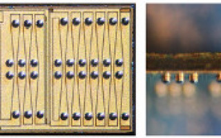
Flip Chip Replaces Wirebond
Another way to improve EMI is to shorten the wires in the hot loop. This can be done by removing the traditional wirebond method of connecting the die to the package pins. In the package, the silicon is flipped and copper pillars are added. This further minimizes the area of hot loops by shortening the distance from the internal FET to the package pin and the input capacitors.
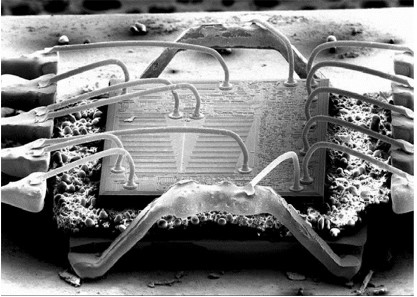
Figure 4. Wirebond shown in a disassembled LT8610.

Figure 5. Flip chip with copper pillars.
Silent Switcher vs. Silent Switcher 2

Figure 6. Typical Silent Switcher application schematic and how it looks on the PCB.
Figure 6 shows a typical application using a Silent Switcher regulator, recognizable by the symmetrical input capacitors at the two input voltage pins. Layout is important in this scheme, as Silent Switcher technology requires these input capacitors are laid out as symmetrically as possible to provide the mutual field cancelling benefit. If not, the benefits of the Silent Switcher technology are lost. The problem, of course, is how does one ensure proper layout in design and all the way through production? The answer is Silent Switcher 2 regulators.
Silent Switcher 2
Silent Switcher 2 regulators take EMI reduction one step further. The EMI performance sensitivity to PCB layout is eliminated by incorporating the capacitors into the LQFN package—VIN caps, INTVCC, and boost caps— allowing for placement as close as possible to the pins. All of the hot loops and ground planes are internal, resulting in minimized EMI, and an overall smaller solution footprint.

Figure 7. Silent Switcher application vs. Silent Switcher 2 application diagrams.

Figure 8. Decapped LT8640S Silent Switcher 2 regulator.
Silent Switcher 2 technology also results in improved thermal performance. The large, multiple-ground exposed pads on the LQFN flip-chip package facilitate the extraction of heat from the package into the PCB. Higher conversion efficiency also results from the elimination of high resistance bond wires. When tested for EMI performance, the LT8640S passes CISPR 25 Class 5 peak limits with a wide margin.
µModule Silent Switcher Regulator
Taking the knowledge and experience gained while developing the Silent Switcher portfolio and coupling it with an already vast µModule® portfolio allows us to deliver a power product that is easy to design while meeting some of the most important metrics of a power supply—thermal, reliability, accuracy, efficiency, and great EMI performance.
Figure 9 shows the LTM8053 incorporating the two input caps, allowing for magnetic field cancellation, as well as a number of other passive components required for this power supply to operate. All of this is achieved in a 6.25 mm × 9 mm × 3.32 mm BGA package, which allows customers to focus their efforts on other areas of their board design.

Figure 9. LTM8053 Silent Switcher exposed die and EMI results.
Removing the Need for an LDO Regulator—Power Supply Case Study
A typical high speed ADC requires a number of voltage rails, and some of those rails must be very quiet to achieve the ADC’s highest data sheet-listed performance. The generally accepted solution to achieving a balance of high efficiency, small board area, and low noise is to combine switching power supplies with LDO postregulators as shown in Figure 10. Switching regulators are able to achieve relatively high step-down ratios with high efficiency, but are relatively noisy. A low noise LDO postregulator is relatively inefficient, but it can reject much of the conducted noise produced by the switching regulator. Efficiency is helped by minimizing the step-down ratio of the LDO postregulator. This combination produces clean supplies, resulting in the ADC operating at top performance levels. The problem is a complex layout of numerous regulators, and LDO postregulators can have thermal issues at higher loads.

Figure 10. Typical power supply design for powering an AD9625 ADC.
In the design shown in Figure 10, several trade-offs are evident. In this case, low noise is a priority, so efficiency and board space must suffer. Or, maybe not. The latest generation of Silent Switcher µModule devices combines low noise capability switching regulator design with µModule packaging—achieving a heretofore unachievable combination of easy design, high efficiency, compact size, and low noise. These regulators minimize board area, but also enable scalability—several voltage rails can be powered from one µModule regulator, providing further area and time savings. Figure 11 shows an alternative power tree using the LTM8065 Silent Switcher µModule regulator to power the ADC.

Figure 11. Space saving solution to powering the AD9625 using a Silent Switcher µModule regulator.
These designs have been tested against each other. ADC performance using the power supply designs in Figure 10 and Figure 11 have been tested and compared in a recent article published by ADI.1 Three configurations were tested:
- A standard configuration using a switching regulator and an LDO regulator to power the ADC.
- Using the LTM8065 to directly power the ADC with no further filtering.
- Using the LTM8065 with the addition of an output LC filter to further clean the output.
Measured SFDR and SNRFS results showed that the LTM8065 could be used to power the ADC directly without compromising the performance of the ADC.
The core benefit of this implementation is a significant reduction in the number of components resulting in higher efficiency, far easier production, and reduced board area.
Summary
In conclusion, as we see a shift toward more system-level designs with ever more stringent specifications, it is important to utilize modular power supply designs where possible, especially where there is little power supply design expertise. With many market segments requiring that the system design pass the latest EMI specifications, the use of Silent Switcher technology is integrated into the small form factor, and ease of use of a µModule regulator can drastically improve your time to market while saving board area.
Advantages of Silent Switcher µModule Regulators
- Saves PCB layout design time (no need to respin the board to rectify noise issues).
- No need for additional EMI filters (saving cost on components and board area).
- Reduces the need for an in-house power supply expert to debug the power supply noise.
- High efficiency at wide operating frequency range.
- Can remove the need for an LDO postregulator when powering noise-sensitive devices.
- Shortened design cycle.
- High efficiency in a minimal board area.
- Good thermal performance.
References
1 Aldrick Limjoco, Patrick Pasaquian, and Jefferson Eco. “Silent Switcher µModule Regulators Quietly Power GSPS Sampling ADCs in Half the Space.” Analog Devices, Inc., October 2018.
About the Author
Bhakti Waghmare is currently a product marketing engineer for the μModule Regulator Power by Linear Product Group based in Santa Clara, California. She supports marketing for μModule regulator power products. Bhakti joined Analog Devices in 2018. She attained a B.S. in mechanical engineering and an M.S. in industrial engineering from Wayne State University, Detroit, MI. She can be reached at [email protected].
About the Author
Diarmuid Carey is an applications engineer with the European Centralized Applications Center based in Limerick, Ireland. He has worked as an applications engineer since 2008 and joined Analog Devices in 2017, providing design support for the Power by Linear portfolio for European broad market customers. He holds a bachelor’s of engineering in computer engineering from University of Limerick. He can be reached at [email protected].