eFPGA: Taking the Cost, Size, and Power Consumption out of FPGA Without Sacrificing Speed or Programmability
June 02, 2023
Blog
Over the years, FPGAs have made their way into a wide variety of applications – starting from low-volume applications and migrating their way into high-growth areas such as cloud data centers and communications systems. Programmability is key in many situations where algorithms, standards, and customer needs are rapidly changing. However, this advantage has also come at a cost, because FPGAs are power-hungry and take up valuable space.
Now flash forward to 2023, and chip designers are finding out that it does not have to be this way. The capability now exists to integrate the FPGA, which not only eliminates the expensive FPGA package, but also gets rid of the power-hungry SerDes/PHYs. With these two things gone, customers can simply take what is left (the digital logic) and embed it into an SoC like they would with an Arm or RISC-V processor. Many companies have already done this and have working silicon now.
While one might think they lose something by getting rid of the packaging, the opposite is true. In fact, you gain two key things with embedded FPGA (eFPGA):
- eFPGA can deliver the same speed and density as the FPGA it is replacing as long as it’s in the same process node. And fortunately, the leading eFPGAs are available in 7, 12, 16, 22, 28 and 40 nm process nodes, with 5nm in development.
- Unlike FPGAs that come with a limited number of sizes and a fixed ratio of logic/DSP/RAM, eFPGA lets chip designers get the exact size they want with the exact amount of logic/DSP/RAM they need in any process node. With this flexibility, they can choose to implement a few thousand LUTs to millions of LUTs.
An eFPGA Case Study
Over the last several years we’ve seen eFPGA adoption starting to really take off. Companies that have started using it include Renesas, Boeing, Datang Telecom, Sandia Labs, DARPA, DoD, AFRL, and many more are that choose to stay confidential or are in the design phase. Renesas is a perfect example of a company that has proven that FPGAs don’t need to be big, power hungry and expensive. Their Forge family FPGAs are tiny, consume milliwats and are expected to sell in volume at prices less than 50 cents.
Using eFPGA, the ForgeFPGA family is able to provide relatively small amounts of programmable logic that can be quickly and efficiently designed into cost-sensitive applications using a very small package just millimeters on a side.
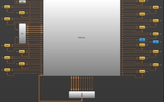
Here is the top level view of the ForgeFPGA in their GUI (from a document on their website):

The FPGA core is an eFPGA tile/array that connects directly to GPIOs, BRAM, PLL, etc. The user generates the code that runs on the FPGA.
Below is a screenshot of P&R results:

Finally, below is an example of an IP block in their GUI:

Markets and Applications
One of the key benefits of integrating FPGA into an SoC is that it can cut power and cost 5-10x while maintaining full speed and flexibility. Customers can use eFPGA for glue logic functions for GPIO or for certain parts of the SoC that may need to be updated in the future due to changing requirements, protocols, and algorithms. They can also use it to build in the option of doing post-silicon bug fixing.
Some companies might choose to build Renesas-type micro FPGAs with super low power, while others may use it on the compute bus. This latter approach provides a programmable co-processor that implements workloads like compression and encryption that use FPGA’s parallelism to run much faster than the host MPU.
We have also found that in many cases the best power/performance/area comes from hardening the data path in the FPGA. With the data path hardened, customers can then use eFPGA as the control path. This produces a very high performance state machine that controls the configuration and the execution of the data path and can run at 533MHz worst case in 16nm and 800Mhz in 7nm.
Below are some of the specific applications that we are already seeing eFPGA used in today:
- Space and Aerospace — eFPGA technology allows systems to be smaller, lighter, and consume lower power. More importantly, hardware updates can be made to ASICs while orbiting the planet. In addition, eFPGA can be ported to any fab so manufacturing can be in a location preferable to the aerospace company. The technology can even be radiation-hardened if it is designed using a rad-hard standard cell library. eFPGA can use Rad Hard Standard Cells for storage elements and design rules for clock lines and resets to improve tolerance to Single Event upsets.
- Networking – Smart network interface cards (Smart NICs) often have FPGAs sitting next to the data processing unit (DPU) to support acceleration for encryption/decryption, AI for data analysis, firewall, TCP/IP, HTTP, and compression, etc. With eFPGA, these accelerators can now reside in the eFPGA on the same chip as the Data Processing Unit (DPU), which reduces BOM costs, system power and improves performance. eFPGA has near-hardwired ASIC performance and is also suitable for use in configurable data paths and packet inspection and parsing.
- Wireless Communications – Base stations today are major users of FPGAs for flexibility and reconfigurability to allow for customization and real-time updating of protocols and algorithms for applications such as beam forming and networking.
- Storage – SSD controllers are putting more intelligence into their systems for better data management to analyze compromised (aka worn) memory location to avoid loss of data, leverage AI for data analysis and update to the latest sorting, encryption, and compression algorithms. eFPGA is the ideal programmable solution for these widely different workloads since it can be programmed with any type of hardware accelerator.
- Artificial Intelligence – Data centers use FPGA for AI accelerators. Integrating eFPGA into the main ASIC improves performance by eliminating ASIC to FPGA data latency and system power by removing redundant circuitry that resides on both the ASIC and FPGA such as SerDes and PCI PHYs, etc.
- MCU/IoT – By incorporating a small amount of eFPGA to Application Specific Standard parts (ASSPs) and application processors, chip suppliers can provide their customers the ability to customize their chips while producing a standard product. eFPGA is an ideal security solution for IoT applications because system companies can keep their proprietary circuit design in-house and program the MCU with eFPGA post-manufacturing.
All the Benefits of FPGA without the Excess Baggage
As explained above, FPGAs don’t have to be big, expensive, and consume lots of energy. An eFPGA essentially takes the best of the FPGA, gets rid of the excess baggage, and leaves customers with a solution that can provide all the flexibility of FPGA with the same speed and density they have always used.