Multi Voltage SoC Power Design Technique
September 14, 2022
Blog
Minimizing power consumption is a major factor that contributes to the modern-day development of IC designs, especially in the consumer electronics segment. The heating of the devices, the time it takes to turn on/off the features of handheld devices, battery life, etc are still under reforms. Hence it becomes important that best practices of chip design are adopted to aid the power consumption in SoCs (System on Chip) and other ICs (Integrated Circuit).
According to market Research Future, the global System-on-Chip market was valued at USD 131.83 billion in 2021, and it is predicted to reach USD 214.8 Billion by the end of 2030, with a CAGR of 8.30 % from 2021 to 2030. The performance of the Silicon is greatly influenced by power management for SoCs and RTL designs. To attain power statistics, industries utilize power-aware designs.
This blog's focus is on multi-Voltage design terminology that can be used in HDL coding to determine silicon's power performance. These aid in comprehending the design parameters when putting into practice power-conscious designs.
Multiple Voltage Design (Multi Voltage Power Domain) Method
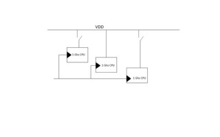
Power supply has a direct relationship with dynamic power which consists of switching & short-circuit power. Therefore, reducing power naturally enhances power performance. The decreased threshold voltage causes an increase in gate delay. Lowering the voltage of SoC blocks is perhaps the first design implementation that is used to meet power performance goals. In Figure 1 the system shows different voltage levels.

Figure 1
Lowering the voltage lowers the current flowing and increases the delay in the gates, and by that means, the designs may not be able to run at desired clock frequencies. Lowering the voltage may cost the performance statistics but the performance can still be met as seen in Figure 1. Here the VLSI chip performance is achieved by lowering individual voltages of different modules.
Figure 1 can also be referred to as a multi-VDD design. The logic is partitioned into different domains called power domains. The structural model or a gate-level netlist derived from behavioral Verilog uses a different voltage line for each domain. The individual domains can be run as per performance objectives. Figure 2 shows an elaboration of the same.

Figure 2
The power intent derived using the IEEE standard 1801-2018 Unified Power Format UPF 3.1 is used by many companies to define the power parameters of a chip. The power architect makes use of this technology to create files that describe the power and power control intent of an electric design. Supply sets, power switches, level shifters, and memory retention techniques are all included in the annotation. Power states, transitions, a collection of sim states, the pg (power/ground pin) type and function properties of nets, and the -update parameter to assist the gradual refinement of the power intent are all definable descriptions of the potential power applied to the electronic system.
Requirements to Create a Multi-Voltage Design
Level shifters
As shown in figure 3, level shifters will shift the level of voltages to ensure different modules operating at different voltages will operate correctly when LS (Level shifter) circuits are attached. The circuits are implemented in HDL, and they can also be made to implement the drive strength. The figure shows a low to high voltage level shifter (A) and a high to low voltage level shifter (B). Vi and Vo are the sources and destinations of different voltage levels in different modules.

Figure 3
Power gating
The method in figure 4 is referred to as 'disconnecting the power of the gates which are not in use'. The figure shows an implementation of such a situation. Power gating is used to reduce leakage power. This step is performed at an architecture level while computing the performance factors of the low power module, or module at a sleep state while other priority modules are ON, or module where power is to be disconnected by software, or while shutting down the power.
Power gating is significantly used with modern-day traditional terms like SLEEP/WAKE events of the device. The wakeup and sleep sequence follow certain architectural decisions to enable or disable a sequence of operations that controls the power logic of the chip.

Figure 4
Special care must be taken while implementing power gating as output signals from a power gated block pose special challenges. This considers isolation and retention strategies at the micro-Architecture level while performing the wake-up or sleep sequence. The placement of circuits of retention and isolation strategy in the circuits should not affect the power performance factors.
Retention cells are used to save the state of the chip to use during the wakeup sequence of a module. Figure 5 shows a state being saved upon the assertion of the saving sequence. Vdd_sw (Switched supply voltage) is controlled by switch and Vdd is always on voltages to power up the circuit. When save (saving sequence) is asserted, the output of the module is latched and is available as feedback.

Figure 5
Figure 6 illustrates where isolation cells are introduced when a shutdown or a sleep phase is isolated from the receiving end. Isolation cells keep them turned off and block output to a predefined value. This way, isolation cells are attached to reduce crowbar currents, thereby reducing power leakage.

Figure 6
Clock Gating
This method is referred to as turning off the clock transitions when the circuit does not encounter switching of internal signals when there is no activity to be performed. This help controls the frequency of transitions from the power equation. Almost all EDA tools identify and support this.
The complexity of SoCs has expanded, introducing new demands for power management. The supply of the various SoC power domains must be flexible enough to be controlled by developers to control power dissipation and improve battery autonomy. Careful power analysis and knowledge of the capabilities of the tools at hand are prerequisites for selecting the best solutions. Power-related crises can be prevented by analyzing power demand as early as possible in the design flow. Power goals are also made simpler to achieve by early analysis because higher-level techniques save the most power.
Sarth Rana is a Senior VLSI Engineer at Softnautics, a microelectronics enthusiast having experience working in RTL designs and verifying complicated ASICs like USB, and PCIe. He has worked on FPGAs, High-speed memory Verification, Functional verification, Low power verification, and Assertion based verification. His hobbies include sketching and reading books.

Sarth Rana is a Senior VLSI Engineer at Softnautics, a microelectronics enthusiast having experience working in RTL designs and verifying complicated ASICs like USB, and PCIe. He has worked on FPGAs, High-speed memory Verification, Functional verification, Low power verification, and Assertion based verification. His hobbies include sketching and reading books.