General-Purpose FPGAs: An Innovation-less Decade
November 24, 2020
Story

Some corners of the electronics universe go years or decades without a significant technology upgrade. Passive electronic components are a good example. Then there?s also embedded programmable logic.
Some corners of the electronics universe go years or decades without a significant technology upgrade. Passive electronic components are a good example, as not much more performance or cost can be pulled out of devices like resistors, at least not without a materials revolution. Another is the battery market, where offerings have by and large been optimized to demand.
Then there’s also the embedded processing space. That’s right, logic. Specifically, general-purpose programmable logic.
In 2011, both Xilinx and Altera (now Intel) released the Artix-7 and Cyclone V GT, respectively. Each of these devices contained fewer than 100K logic cells (50K for the Xilinx part and up to 77K for Cyclone V devices), but delivered a nice mix of I/O flexibility, logic, and low-power consumption in applications ranging from automotive subsystems to industrial automation equipment to communications infrastructure.
And then, nothing. For almost a decade, there were no new devices introduced in the low-power, general-purpose, sub-100K-logic cell class of FPGAs.
Why not? Well, a couple of factors were in play. First, a lot of the end systems that leveraged these devices are long-lifecycle deployments in industries that live by the “if it ain’t broke, don’t fix it” mantra. But the primary reason is that the two major FPGA suppliers strategically transitioned away from traditional embedded markets to capture higher-margin business in environments like the data center, which require devices with 1 million logic cells or more for things like workload acceleration.
In the absence of other competitive offerings, the size, power consumption, I/O speed, I/O density, and soft error rates (SERs) of the Artix-7 and Cyclone V GT remained the status quo for years.
Changing CMOS is the Only Constant
Of course, even in the most static parts of the electronics space, change is the only constant. And change has recently come to the sub-100K logic cell general-purpose FPGA market with Lattice Semiconductor’s Certus-NX line.
Certus-NX FPGAs are available with between 17K and 40K logic cells, and, like the alternatives mentioned earlier, include hardened 5 Gbps PCIe lanes. But while the Lattice devices are comparable across those parameters and even include less RAM and fewer DSP multipliers, they deliver up to 70 percent faster differential I/O speeds, twice the I/O density, and 4x lower power consumption.
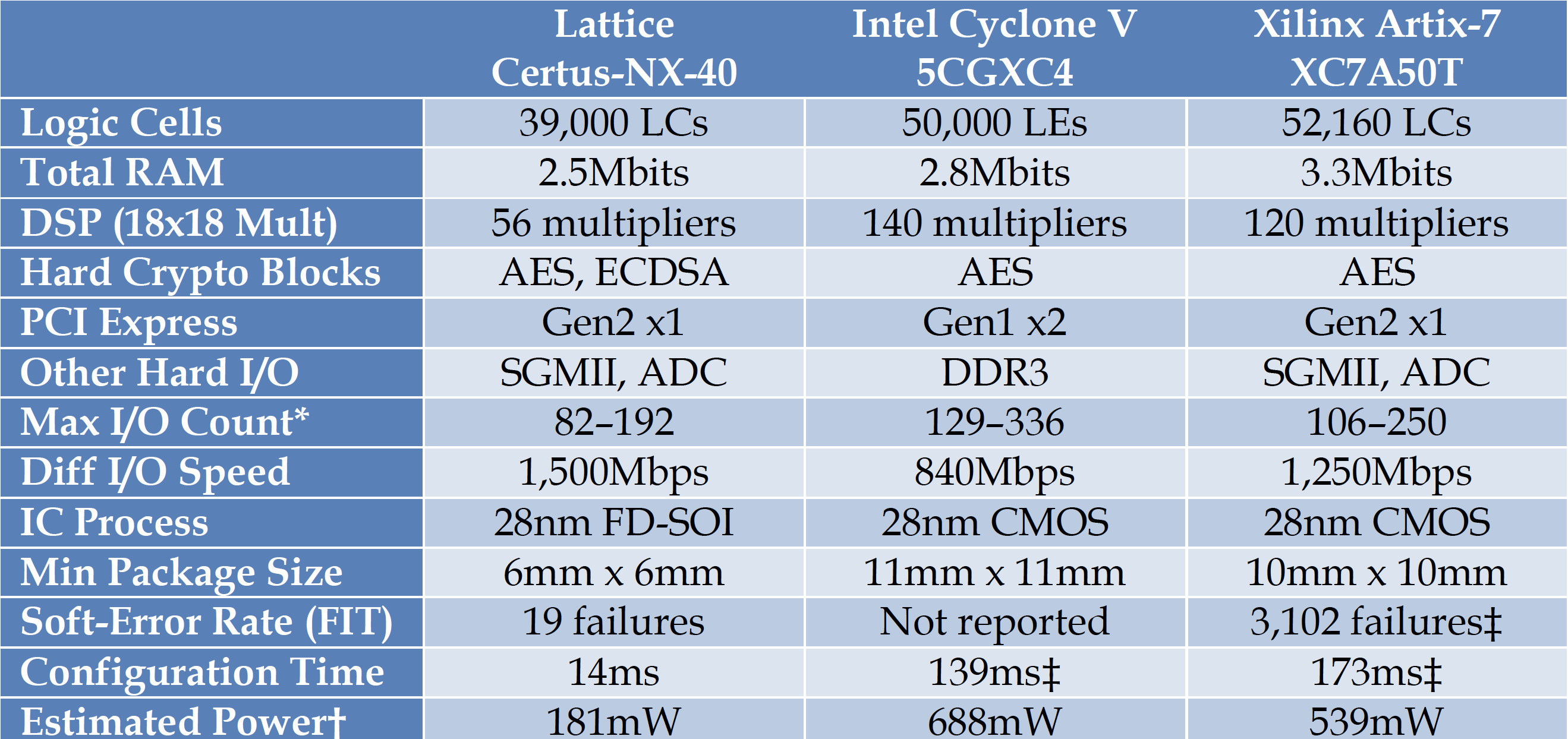
They are also roughly half the size, measuring just 6 mm x 6 mm.
Certus-NX devices achieve these performance and efficiency gains through a trick of Moore’s law. While the Lattice, Intel, and Xilinx FPGAs are all manufactured on 28 nm nodes, the Certus-NX platforms utilize a fully-depleted silicon-on-insulator (FD-SOI) process technology that exhibits less parasitic capacitance than bulk CMOS (Figure 1). This allows for body biasing, or the ability to make transistors more performant or power efficient by passing a programmable voltage across the layer of oxide insulation underneath them.
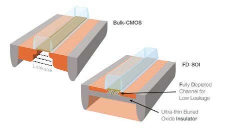
Despite its use of already-established manufacturing techniques, FD-SOI produces smaller die sizes and is higher reliability than standard CMOS. The technology virtually eliminates SERs in SRAM, which contributes to a mean-time between failure (MTBF) on Certus-NX devices that is more than 150x the competition.
Progress for Progress’s Sake
Other modernizations in the Certus-NX include support for ECDSA cryptographic algorithms, and 3 ms I/O configuration and 14 ms device configuration, all of which combine with the aforementioned power savings to offer a solid foundation for connected and battery-operated devices.
But just as important, the size, performance, reliability, and power improvements also represent a significant step forward for traditional embedded applications, be they legacy deployments or new installations. Let’s not forget the global footprint of these systems, and allow progress for the sake of progress to leave us with innovation-less decade.