On the Origin of xSPI by Means of Natural Selection of NOR Flash in AI-Enabled Embedded Systems
July 21, 2026
Blog
Embedded systems have continued to evolve and as this happens, the rate limiting factors have too. In particular, the bottleneck on performance is no longer the processor alone; and memory access is now a critical factor in system responsiveness.
Previously, memory access had been just a secondary consideration across virtually all sectors of embedded applications – from automotive to industrial control. Now, there are new AI product trends that require real-time behavior (and user experience) and these are directly affected by the ability to access code and data quickly.
While changes in NOR flash are happening at a slower rate compared with processing power, evolutions continue in memory, with the steady shift from traditional SPI NOR Flash to the higher bandwidth xSPI.
Memory as the Bottleneck
Flash is used to store not only firmware and boot code but also the algorithms on which embedded operations run. These have become increasingly complex and must be accessed repeatedly throughout the system operation.
Therefore, with ever-increasing demands being placed on embedded workloads, the latencies during memory access begins to matter as much as raw compute capability. This is true for virtually all embedded systems, but the effect takes a remarkable leap when the system is AI-enabled or needs to operate in real-time networks.
The natural points of delay come in the fetching of the code algorithms and the control loop response. These delays need to be minimized further; and what was once acceptable is now a bottleneck on performance.
SPI NOR Flash
In early NOR Flash devices, parallel interfaces were used, which resulted in very large (32-50+ pin) packages. As parallel NOR devices depend on the supported address/data bus plus control signals, it also came with a significant limitation on maintaining pinout/package compatibility when migrating to higher densities.
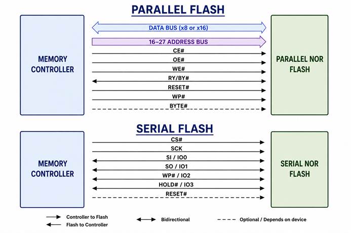
Serial interfaces offered significantly reduced pin counts and enabled far smaller compact packages to be produced, which in turn improved system size, flexibility and overall cost. Accordingly, SPI NOR Flash (serial peripheral interface) gradually replaced parallel connections, becoming the mainstream interface for NOR Flash, but there were limitations.
This system was more than sufficient for many years, with the single-channel SPI storing boot code and parameter data; and being used from system power-up as a code shadowing tool. In code shadowing, the SoC has to fetch the boot code from the SPI NOR and transfer it to RAM, and then perform execute-in-place (XIP) on RAM.
With increasing application performance requirements, the dual-channel, quad-channel, as well as double transfer rate (DTR) SPI NOR memories were developed and introduced. These interfaces improved data throughput and while they still did not quite match the XIP performance of parallel interfaces, they are getting closer. More importantly, these new features enabled XIP code execution directly in the SPI NOR flash, hence the shift from parallel NOR to SPI NOR-based designs accelerated. However, there was still a fundamental limitation that these new solutions could not address and solve.
SPI architectures reached their peak performance capabilities at clock frequencies above 166MHz STR and 80-90MHz DTR and the interface cannot function and operate beyond this point. This meant any applications that needed instant-on, or frequent code execution and rapid algorithm access using these legacy SPI devices can suffer from memory read latency. In turn, these SPI architectures will constrain the system’s overall responsiveness.
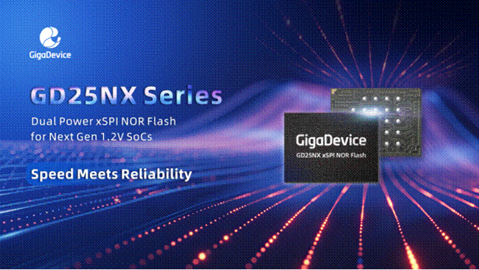
Image caption: The GD25NX xSPI NOR Flash IC
xSPI
Evolutions in the SPI architecture continued, and the creation of xSPI is far from being a minor or incremental update. It gives four additional I/O lines to deliver a byte-wide octal bus (x8). It also adds a support data strobe (DQS) pin to provide a hardware-synchronized timing reference, which allows the controller to sample data at the precise moment it is valid and effectively removes the previous SPI frequency barriers.
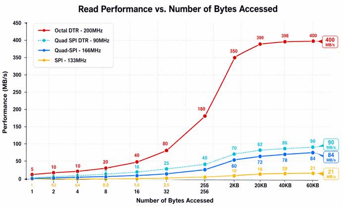
Through these notable upgrades, bandwidth for xSPI is increased to 400 MBytes/s at the maximum (200 MHz) DTR frequency, allowing data throughput transfers that are between 4 and 5X faster than existing SPI NOR solutions.
In short, xSPI represents a structural shift in how SPI NOR Flash interfaces deliver performance, enabling data throughput levels that were previously unattainable with conventional SPI designs.
System Level Benefits
In order to properly assess the impact of xSPI on embedded applications, we need to look beyond the raw interface specifications and focus on the system level operations.
Applications that use an MPU-based AI SoC process code and algorithms frequently by retrieving from external Flash memory during operation in order to compare incoming data to stored models.
If SPI is used, its innate slow responsiveness would make it impossible for the whole system to operate normally or function at all, unless alternative comparative solutions with fast latency are used.
Conversely, the enhanced bandwidth of xSPI interfaces means code and data can be accessed far more quickly and far more consistently than it would be when using SPI. As such, this implementation will lead to systems that are more able to maintain real-time behavior, especially when working with more complex workloads to enable seamless, low-latency performance at scale.
Conclusion
The continued advances in both performance and complexity in embedded systems means SPI bandwidth and latencies are now at a point where they are only auxiliary support for advanced embedded systems with integrated AI. Advanced memory solutions are becoming foundational requirements.
xSPI’s enhanced throughput, efficiency, and support for real-time operation is making it now the baseline interface for high-performance SPI NOR Flash.
This is true across a huge range of technologies and sectors where AI is integrated particularly in automotive, IoT, and industrial applications. The evolution does, of course, reflect a broader industry trend toward faster, more responsive memory architectures and SPI is undergoing a phase of evolution to xSPI. As a result of the benefits it brings, it is the best-suited interface to withstand the conditions required in the AI era.
For more information, visit gigadevice.com.