Finding Efficiency Through Thermal Management and Hard IP
June 11, 2025
Sponsored Blog

A key watchword of electronics design for the last decade has been efficiency. Finding efficiencies in design processes accelerates time to market. Innovations providing more efficient pathways for data, energy, and heat make for lower costs of operation, longer product lifecycles, and reduced environmental impact. None of this is new.
What is gaining much attention is the increased importance of finding these efficiencies. What was once simply forward-thinking has become critical to the success of an enterprise and to the long-term viability of a product in the marketplace.
At the most basic level, chip design has no higher bar for success than efficiency. As chip integration increases, manufacturers need to leverage more advanced thermal management solutions and find novel ways to reduce power consumption. Nowhere is this truer than with high-end FPGAs and SoCs, which are frequently deployed in environments that introduce thermal, electronic, or physical stressors well beyond the consumer electronics norm.
In this article, I look at some of the innovations fielded by AMD in chip architecture and thermal management and discuss how these innovations enable developers to deliver more streamlined and efficient products.
Thermal Solutions
Chips are becoming increasingly more complex, and at the same time, die area is decreasing with each new process node. Furthermore, modern applications demand higher performance, and chips are running at ever faster clock rates. The net impact of all of this is that power density is increasing, and heat must be moved more efficiently.
AMD recently published a white paper on their advances in lidless packaging technology. Leveraging these novel innovations dramatically improves heat transfer, leading to reduced power consumption, product cost, size, and weight. This also means that developers can deploy their designs across wider ambient temperature ranges, which in some applications is the most critical vector for thermal performance.
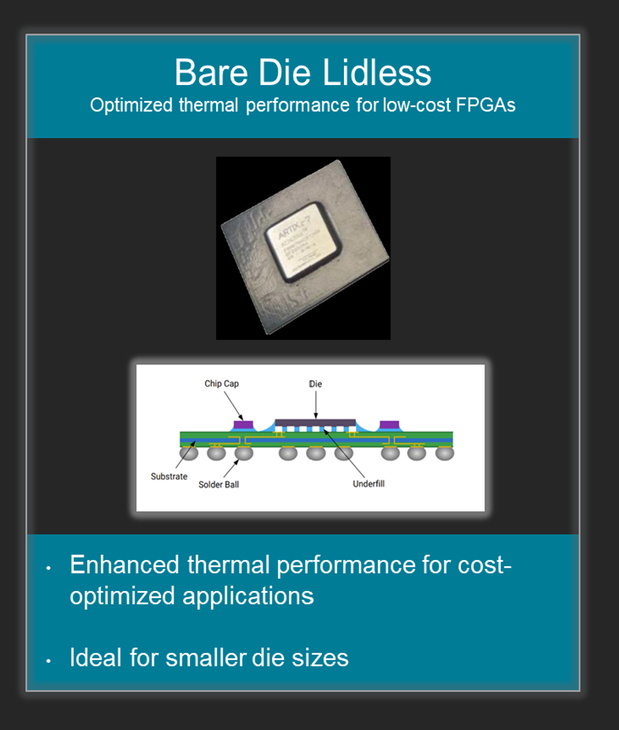
In lidless packages, both the lid and one layer of thermal interface material are removed from the thermal path, and the top side of the die is exposed so that it may be directly mated with a customer-crafted thermal solution. This has advantages, one of which is developers can optimize their thermal management solution in ways that are not possible with lidded packages. In addition to the reduced number of thermal layers, exposing the die allows developers to select a Thermal Interface Material (TIM) that is best for their application. Furthermore, developers can remove the heatsink to inspect and perfect TIM coverage during the pre-production stage—and at other stages of the product lifecycle. This can be crucial for applications designed for extreme levels of reliability.
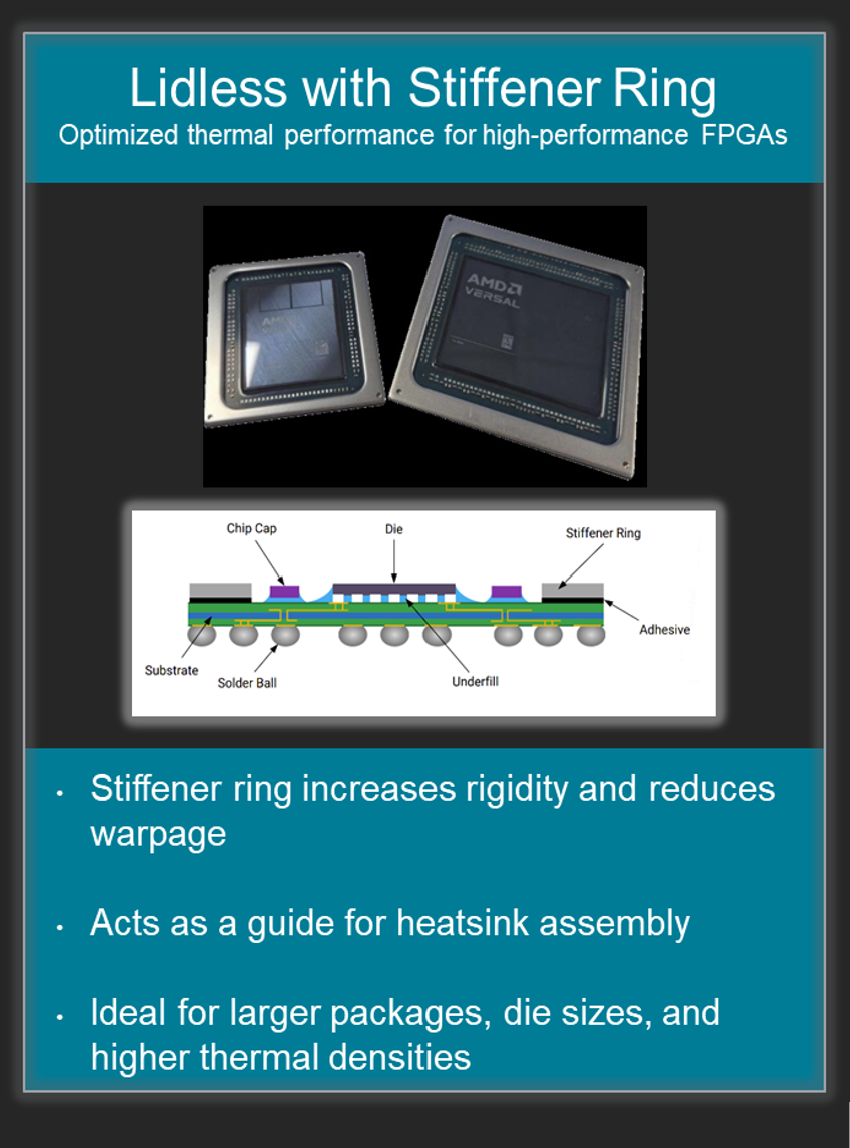
Chips, as with all things manufactured from materials that have differing coefficients of expansion, tend to warp over temperature extremes. Of course, the larger the die and package, the more pronounced warpage becomes. For cost-optimized FPGAs and adaptive SoCs, this does not present a problem because the die and package are comparatively small. However, for high-end FPGAs, the horizontal offset due to warpage is more pronounced, a problem compounded by the fact that high-end FPGA designs are often deployed in more demanding environments. With lidded packages, warpage is much less a problem as the lid acts to stiffen the overall assembly. AMD developed “lidless with stiffener ring” packages to emulate the structural benefits of the lid. In AMD lidless with stiffener ring packages, the periphery of the top of the package integrates a stainless steel “ring” (which is square / rectangular in shape) while leaving the top surface of the die exposed. The below images contrast the two package types:
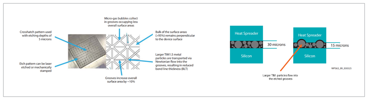
AMD also patented and pioneered the use of a novel heatsink etch pattern, intended primarily for use with lidless packages and Phase Change Material (PCM) TIMs. The concept behind this etch pattern is that machining the surface of the heatsink with a crosshatch reduces the thickness of the TIM layer between the die and the heatsink, resulting in improved thermal performance. AMD provides a mechanical design drawing for this pattern, and grants license to AMD customers to use these etch patterns exclusively with AMD FPGAs and SoCs.
 John Heslip, a Senior Technical Marketing Manager at AMD, says that the proven AMD lidless design manages thermal concerns so well that in one use case there was a 24°C reduction with about a 50 percent reduction in static power (see the white paper). This is the sort of power and thermal advantage that would be tough to achieve through innovations in semiconductor process or RTL design optimization.
Hard IP and the AMD programmable Network on Chip
Another area where AMD has consistently innovated is in the integration of hard IP. You may have read my previous article discussing the AMD Versal RF Series (adaptive SoCs) in which I shared the significant SWaP advantages that integration of hard IP can offer. But in the context of this article, the focus is on one specific hard IP innovation – a programmable network on chip that provides connectivity between all major blocks on the silicon.
While some FPGA manufacturers have chosen only to harden network on chip connectivity in specific devices or families or along a single axis on the chip, the AMD programmable network on chip (NoC) is available in all AMD Versal adaptive SoC devices and carries traffic along both horizontal and vertical axes of the chip. The NoC provides a superhighway for on-chip traffic. Because the NoC is designed to encapsulate and carry AXI traffic from one region of the chip to another, and because virtually all modern FPGA designs leverage AXI, implementing this connectivity as hard IP is a huge advantage. The AMD programmable NoC connects the processing system, programmable logic, DDR memory controller, and other hard IP in the device. This, according to data presented in the AMD NoC white paper, means that data flow across the entire chip is enhanced. Furthermore, as AMD has highlighted in the white paper, the programmable NoC can help developers achieve reduced latency, programmable logic resource utilization, design build times, and system-level power consumption. It is also suggested in the white paper that designs that heavily use the programmable NoC may see an additional benefit – a reduction in the density of the adaptive SoC required for the design.
Although network on chip is quite mature as a technology, AMD has recently released the “modular NoC flow.” Simply put, this workflow enables direct RTL integration of the NoC. Anthony Eid, a Technical Marketing Manager at AMD, said that customers needed a good way to enable RTL flows for the NoC. Now, with the modular NoC flow, the developer can instantiate the endpoints and define constraints for the NoC in RTL. Anthony said that this development was frequently requested by traditional RTL engineers who prefer to live and breathe VHDL or Verilog.
Another key advantage of the NoC is the impact it has on design build time, which translates directly to the number of design iterations the developer can do in a day. If the developer leverages the NoC, the AMD white paper benchmarks suggest that AMD build times can be reduced by up to 50 percent. This is all about developer productivity and will reduce time to market, an efficiency metric that can make or break any project. While not specifically related to the NoC, AMD has also recently introduced “advanced flows” for Versal adaptive SoCs, which also reduce build times – AMD is evidently very committed to improving developer productivity.
It is no big shock that efficiency in design and operations can lead to better outcomes, but the bigger challenge is often the limitations imposed by physics. AMD innovations such as lidless packaging with stiffener ring, etch patterns, and the integration of a hard IP programmable NoC show that these physical limitations can be flexed to achieve truly impressive improvements. Here’s to the next evolution!