A Comprehensive Digital Twin Environment and Semiconductor Lifecycle Management Can Ensure Reliable Data-Center Operations
November 24, 2025
Blog

A growing number of semiconductor applications now require extremely reliable operation. In automotive for example, semiconductors are the underpinning technology for software-defined vehicles and make possible the advanced and self-driving features, which means they are an integral part of safety and critical systems.
For semiconductors used in data center systems that are undergoing increasing software workloads especially with the huge training burden for AI large language models, it’s critical for these systems to stay functioning correctly 24/7 because a failure causing a restart imposes a huge cost on the service operators.
The ever-increasing computing demand is pushing solutions that were typically done during manufacturing design-for-test processes into the entire silicon lifecycle, including in-system and in-field structural testing. At advanced technology nodes, especially those at 7 nm and below with 3D multi-die packaging, we are seeing new complex parametric defects and reliability risks related to aging.
Data center service providers have reported silent data corruption errors caused by subtle chip defects (https://www.nytimes.com/2022/02/07/technology/computer-chips-errors.html). They are producing faulty results only occasionally which makes them extremely difficult to find. A closer examination of the problem has revealed underlying issues test escapes caused by marginalities as well as latent or aging defects, early-life failures, random defectivity, and environmental conditions that led to malfunction.
All these considerations are leading to a rapid growth of a new field called silicon life management (SLM). In which manufacturing testing techniques are used throughout the lifecycle of the device. However, taking these testing techniques from the well-controlled stable manufacturing environment into different real-life dynamic environments poses new challenges but also offers benefits. For example, value of the data collected from running these tests in-field is enhanced because the results can now be associated with environmental conditions.
In addition to in-system structural test, a critical element of SLM is functional monitoring. Key elements of any functional design can be monitored during in-field operation, providing critical data which can be analyzed off-chip.
This data can be collected across an entire fleet of devices; for example, we are seeing data centers deploying hundreds of thousands of GPUs to build an infrastructure to handle aggressive AI-based workloads. These devices are forming systems that must remain 100% functional, working under load for days if not weeks at a time. Therefore, the operation of the SLM elements in the design must be fully understood to ensure that they have no negative effects on the systems’ functional operation and overall performance, but also to fully understand the data that can be collected and how that data can be used.
To do this pre-silicon, a complete digital twin of the system can be created. Given the size and complexity of such systems, performing even basic operations in a digital simulation environment is a challenge but needs to be done. The interaction between the functional design under a representative workload and the SLM infrastructure can be simulated to create a baseline of example data showing variability of the data which is available to aid with system monitoring. In such cases hardware emulation can be used (for example, using Siemens Veloce platform).
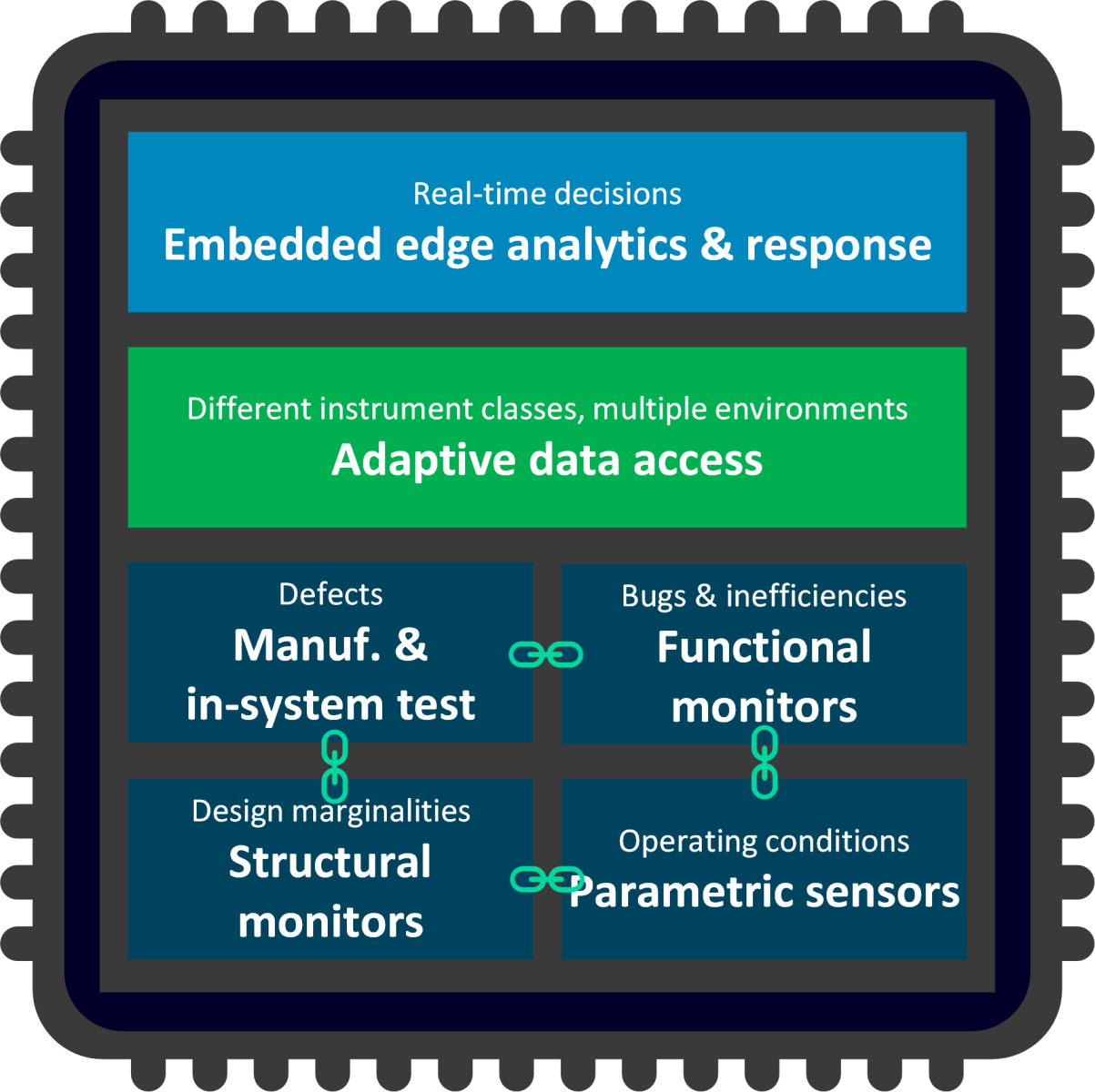 With this complete digital twin of such a system, the full capabilities of the digital elements within the SLM infrastructure can be verified and exploited to extract operation and performance data. This pre-silicon data can be used to drive further enhancements to the functional infrastructure that will improve performance and overall operation. Siemens Tessent software has the various SLM elements built onto a single infrastructure, which can collect data from both the monitor and test instruments within a design, making full alignment of SLM data possible: meaning that anomalies detected by the functional monitors can be directly linked to specific test data delivered at that specific time. This level of data alignment could provide a deeper understanding of the silent data errors that are having a significant impact on day-to-day services through the internet that we’ve come to expect. The digital twin used in SLM can also give a more detailed view of the silicon’s operational health, which is critical to the high demand for 24/7 operation of today’s AI data centers.

Lee Harrison is the Director of Product Marketing for the Siemens Tessent Division of Siemens EDA. He has over 25 years of industry experience working on design-for-test (DFT) related technology. Now with a focus on safety and security, Lee is working to ensure that current and future DFT technologies meet today’s evolving requirements. Lee holds a Bachelor of Engineering (Beng) in MicroElectronic Engineering from Brunel University, London.