Optimizing LDO Headroom Control with a Current Referenced Switching Regulator Design—Part 1: Noise Sources, Impact, and Strategies
December 02, 2025
Blog
This article explores the various sources of noise in switching regulators and their impact on different analog signal chain components. It highlights several noise mitigation strategies, including the use of low dropout (LDO) regulators as effective postregulation filters. The article also shows a range of solutions from Analog Devices (ADI) that deliver optimized LDO efficiency across varying load conditions and output voltages, while pairing good power supply noise rejection. One solution offers a new method for LDOs to control the headroom provided by switching regulators with current reference architectures.
Introduction
Designing an efficient and low-noise power solution is essential for noise-sensitive systems that utilize high-performance analog signal chains. However, noise sensitivity varies between systems and across different frequency ranges. Some applications, such as ultrasound imaging, are particularly susceptible to low-frequency or 1/f noise. Systems with high-performance data converters are notably vulnerable to intermodulation distortion, where fundamental output ripple can interact with the carrier signal, generating sum and difference products. These unwanted frequency sideband components can significantly degrade both the signal-to-noise ratio (SNR) and the spurious-free dynamic range (SFDR) of the data converter. Additionally, electromagnetic interference (EMI) is a critical factor, especially in systems that must comply with stringent EMI standards and certifications.
Figure 1 shows the noise frequency spectrum of a typical buck regulator operating in steady-state pulse width modulation (PWM) operation.
Additionally, the fundamental ripple and its harmonics introduce strong spurious energy across the noise spectrum. The fundamental ripple refers to the residual AC voltage present at the output of a switching regulator. It is coherently correlated with the regulator’s switching operation, with its fundamental frequency matching the switching frequency of the converter. This artifact can significantly impact data converters by modulating the analog input carrier, resulting in unwanted sidebands that degrade both SFDR and SNR performance, as shown in Figure 3.
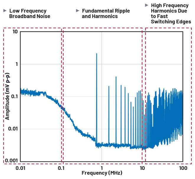
Figure 1. Buck regulator output spectrum.
Typical buck regulators typically generate low-frequency broadband noise that primarily originates from reference noise. This can lead to phase noise issues in sensitive RF components, such as wideband phase-locked loop (PLL) synthesizers with an integrated voltage-controlled oscillator (VCO), as shown in Figure 2.
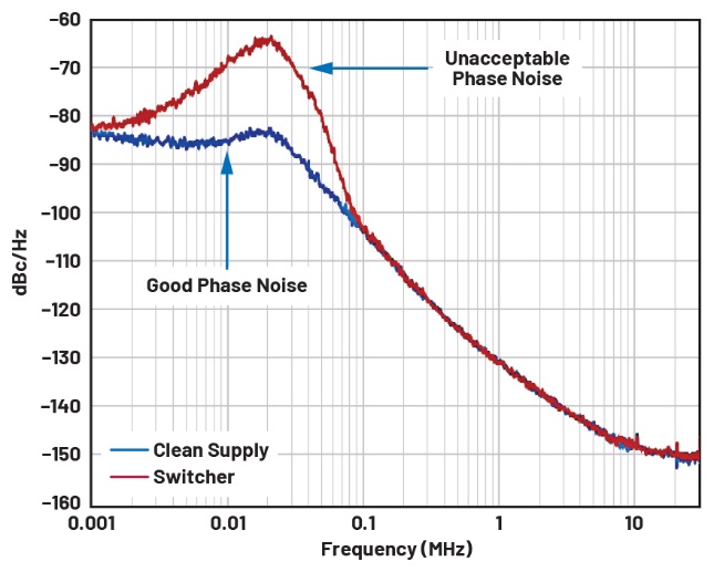
Figure 2. Phase noise of a wideband PLL synthesizer with an integrated VCO.
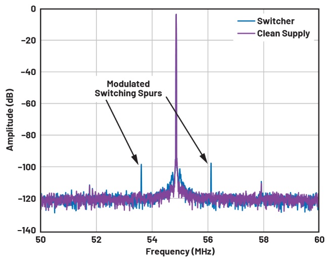
Figure 3. 16-bit, 125 MSPS high-speed ADC fast Fourier transform.
A third noise region involves high-frequency harmonics, which arise from voltage ringing at the switch node. This ringing is caused by the combination of fast switching transitions (di/dt) and parasitic inductance within the regulator’s input loop, as shown in Figure 4, further contributing to EMI and signal integrity challenges, which can be parasitically coupled to the regulator’s output.
Addressing Noise Issues
Low-frequency noise, particularly in the 1/f, is effectively addressed by the Silent Switcher® 3 (SS3) architecture, which offers excellent noise performance in this region.
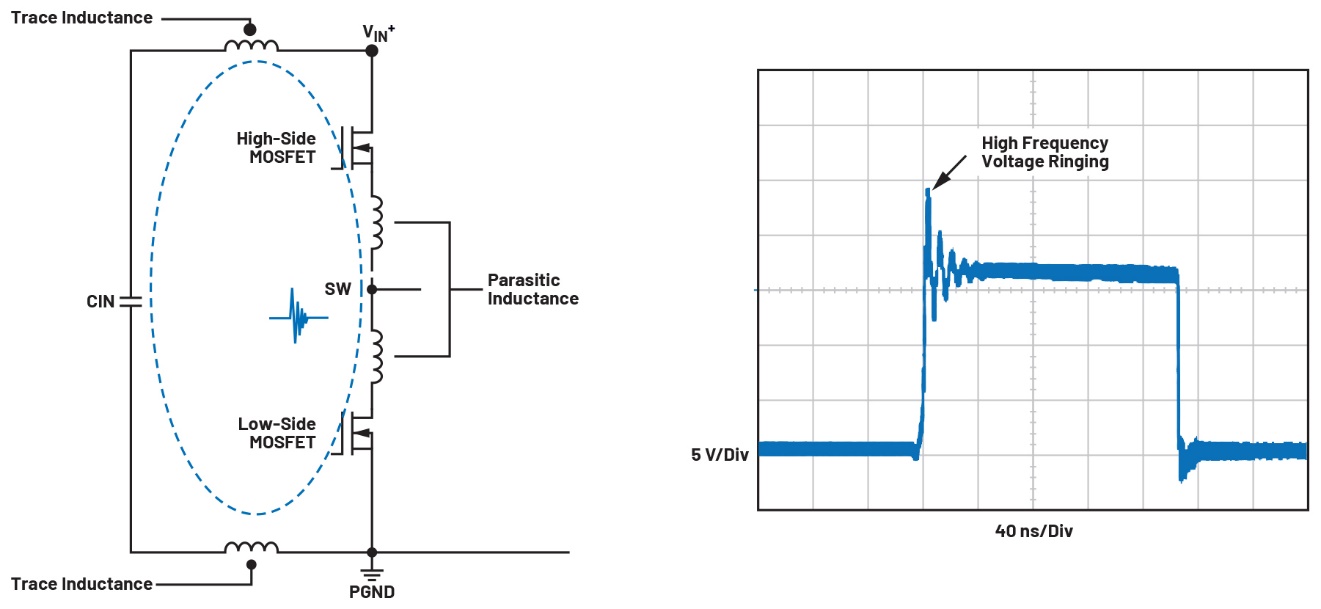
Figure 4. Buck regulator’s input current loop and switch node voltage waveform.
Fundamental ripple can be mitigated using several techniques. One approach is the use of an RC filter, which is simple but comes with certain trade-offs. To achieve a sufficiently low 3 dB cutoff frequency that effectively attenuates ripple, a large capacitor © and a small resistor (R) are needed. However, this configuration can lead to considerable power loss due to the series resistor, making it less efficient for many applications. That said, it may still be acceptable in scenarios where the supply current is relatively low. While the rolloff rate is limited to 20 dB per decade, a key advantage of this method is that it does not require any magnetic component.
An LC filter is also a common and efficient approach. The cutoff frequency is typically designed to be at least a decade below the switching frequency. It offers a steeper rolloff of 40 dB per decade, providing better attenuation. However, designing an LC filter requires careful attention, particularly to resonance effects, which can unintentionally amplify noise at specific frequencies instead of attenuating it. Both passive filter approaches will impact voltage output accuracy and transient performance. Figure 5 depicts the placement of RC and LC filters following the output stage of a switching regulator.
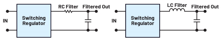
Figure 5. RC and LC passive filters.
An LDO with a high gain bandwidth product (GBW) can effectively reject fundamental ripple in the megahertz range while also delivering excellent low noise performance. However, tradeoffs such as maintaining an adequate power supply rejection ratio (PSRR) and overall efficiency must be carefully considered. Using an LDO as a post-regulation stage offers advantages over passive filters, including improved output voltage accuracy and better transient response. To achieve an optimal solution, it’s important to carefully balance the VIN – VOUT headroom with the LDO’s PSRR characteristics. High frequency harmonics—typically in the range of 100 MHz and above—can be effectively attenuated using ferrite beads. These components exhibit resistive characteristics at targeted high frequencies, making them well-suited for suppressing such high-frequency noise. However, it’s important to note that ferrite beads come with certain complexities, such as resonance effects and impedance variations under different load conditions. These factors must be carefully evaluated during design.1
To achieve superior high-frequency noise performance, Silent Switcher architectures can be utilized. These designs effectively minimize EMI by significantly reducing high-frequency ringing at the switch node, making them a highly robust solution for noise-sensitive applications.
Switching Regulators Utilizing LDOs to Enhance Output Noise Performance
LDOs are commonly used after a switching regulator for post-regulation to filter out noise artifacts at certain frequency ranges. LDOs are typically very effective at rejecting low-frequency noise, often up to several hundred kilohertz. However, high-gain bandwidth LDOs, such as the LT3045, extend this capability into the megahertz range, offering superior PSRR performance. This device is a 20V, 500mA high-performance, ultralow noise, and ultrahigh PSRR regulator, making it ideal for noise-sensitive applications. Compared to passive filters, LDOs offer several advantages, including higher output voltage accuracy, enhanced stability, and superior transient response.
One of the key parameters of an LDO used as a postregulation filter is its PSRR. PSRR quantifies how effectively the regulator suppresses or attenuates noise present on the input supply across a range of frequencies, preventing it from propagating to the output and compromising voltage integrity.
However, PSRR is a function of both load current and headroom voltage, the difference between input voltage and output voltage. Load current plays a crucial role in influencing the open-loop gain of an LDO’s error amplifier, and thus directly impacts its PSRR performance. Under light load conditions, the pass element exhibits higher impedance, which shifts the pole formed with the output capacitor to a lower frequency. This shift enhances the LDO’s ability to reject power supply ripple more effectively.
In contrast, under heavy load conditions, the error amplifier’s output impedance decreases, along with its open-loop gain. This reduction in gain leads to a drop in PSRR, particularly in the frequency range between DC and the unity-gain bandwidth of the feedback loop.
As headroom decreases, the gain of the error amplifier is reduced, and this effect becomes more pronounced with increasing load current. As a result, PSRR performance deteriorates under these conditions.2
LDOs are highly effective as postregulator filters, but their performance is closely tied to both voltage headroom and load current, which must be carefully managed. While increasing headroom can improve power supply ripple rejection, it also leads to greater power dissipation, especially at higher load currents, resulting in reduced efficiency. System designers can strike an optimal balance between effective noise filtering and sufficient voltage headroom to maintain high efficiency. This balance is key to achieving both performance and power-saving goals in the overall design.
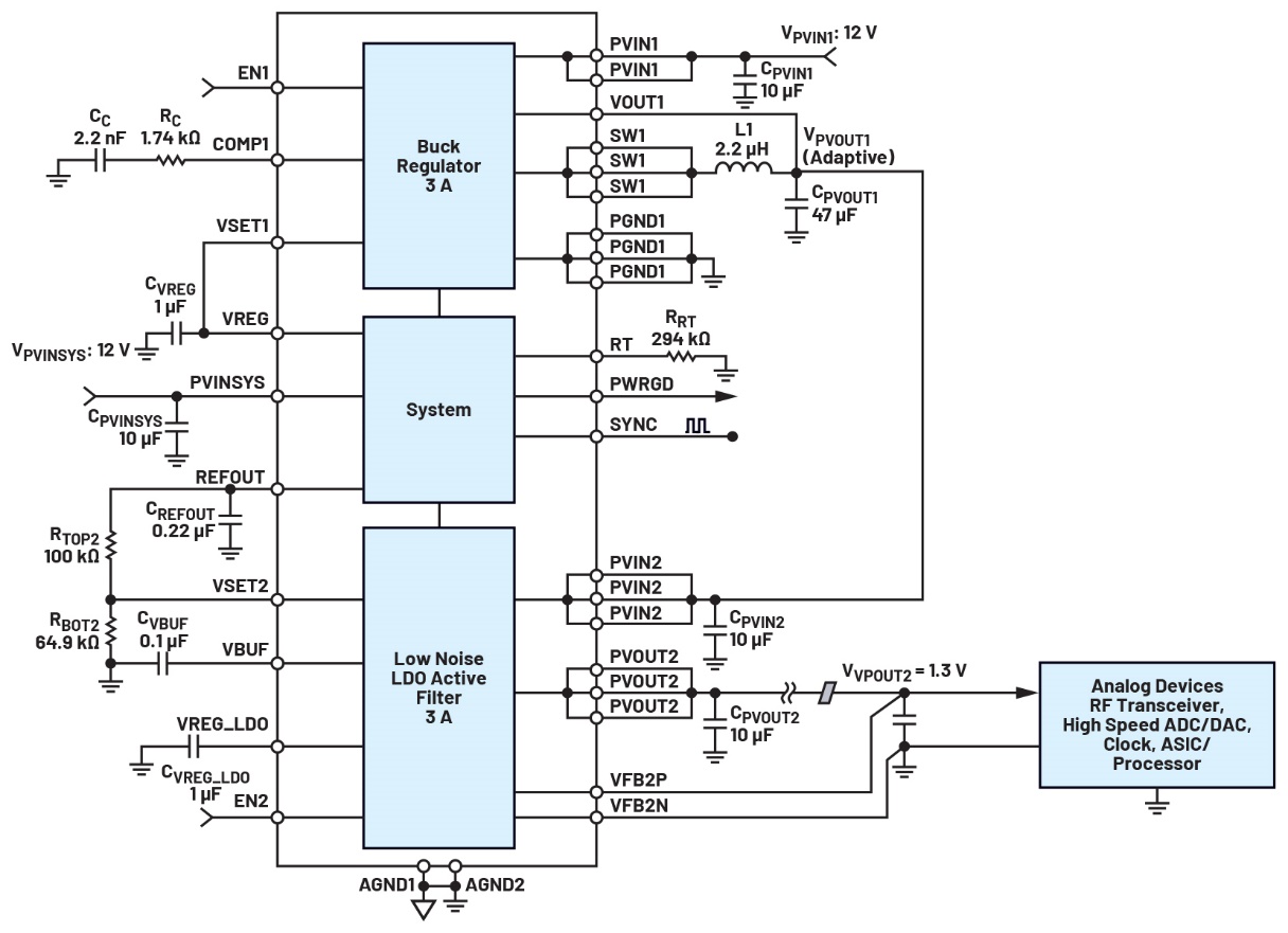
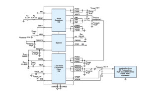
Figure 6. Functional block diagram.
Optimizing Efficiency and PSRR Performance
One approach is based on the dynamic changes of the load current. The ADP5003 low noise micropower management IC integrates a high efficiency 3 A buck regulator on the first stage of conversion, followed by an ultralow noise 3 A LDO, to remove the switching ripple and noise. It offers an adaptive headroom control configuration that delivers enhanced efficiency and thermal performance while minimizing noise suited to high-speed data converters and RF transceivers. Figure 6 shows the functional block diagram of the ADP5003 for adaptive headroom control.
In adaptive mode, the LDO dynamically adjusts its headroom by internally regulating the buck converter’s output voltage based on the LDO’s load current. This ensures optimal efficiency and noise performance. Alternatively, the ADP5003 can operate in independent mode, where the buck and LDO function separately with their output voltages set individually using external resistor dividers.
Figure 7 shows adaptive headroom control for the whole range of the LDO load current. The x-axis is the load current, while the y-axis is the headroom voltage of the LDO.
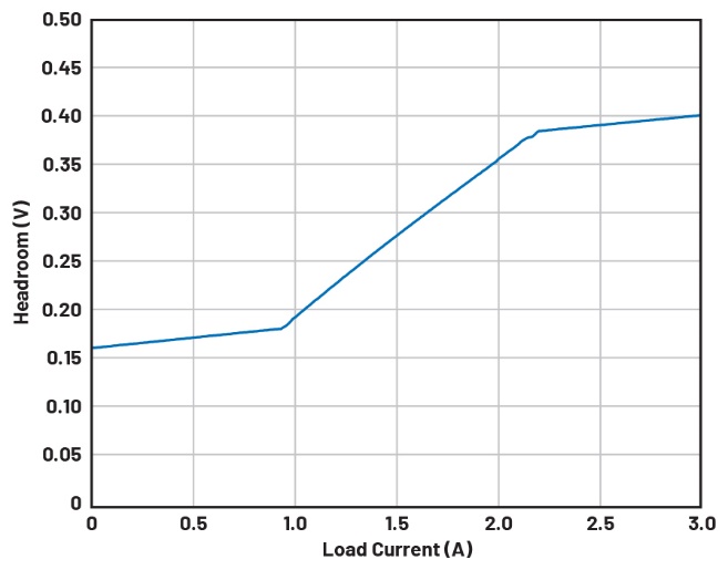
Figure 7. Adaptive mode headroom vs. load current.
The headroom profile in adaptive headroom control is configured to maintain a consistent PSRR across varying load conditions while also enhancing the overall system efficiency. This is shown in Figure 8.
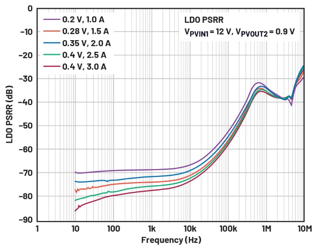
Figure 8. LDO PSRR vs. frequency.
Another approach is based on dynamic changes in VOUT. Voltage input-to-output control (VIOC), a key feature in select ADI LDOs, improves system efficiency by automatically adjusting the switching regulator’s output to maintain a defined headroom voltage. While VIOC does not automatically select the best PSRR, users can manually define the headroom voltage to achieve the desired PSRR performance for specific applications.
An example is the LT3045-1, which has a VIOC feature. This device is a 20V, 500mA, ultralow noise, ultrahigh PSRR linear regulator. Figure 9 illustrates a typical VIOC application, where it is used to postregulate the output of the LT8608 buck regulator. The VIOC voltage is configured to 1 V, with the LDO’s maximum input voltage limited to 16.5 V. It also illustrates how the input-to-output differential voltage can be easily configured using resistor dividers, allowing designers to tailor the balance between PSRR and power dissipation to suit specific application requirements.
Simple LDO Headroom Control Using Switching Regulators with Current Reference Architecture
Current reference architecture is a design approach where a precise current source, rather than a traditional voltage reference, serves as the core element for regulating the output voltage. It has a unity-gain error amplifier, and the output voltage can be easily set by a single resistor. The approach is particularly advantageous in linear regulators and is increasingly being adopted in switching converters to meet the demands of high-performance applications. This can be seen in Figure 10 from a buck IC.
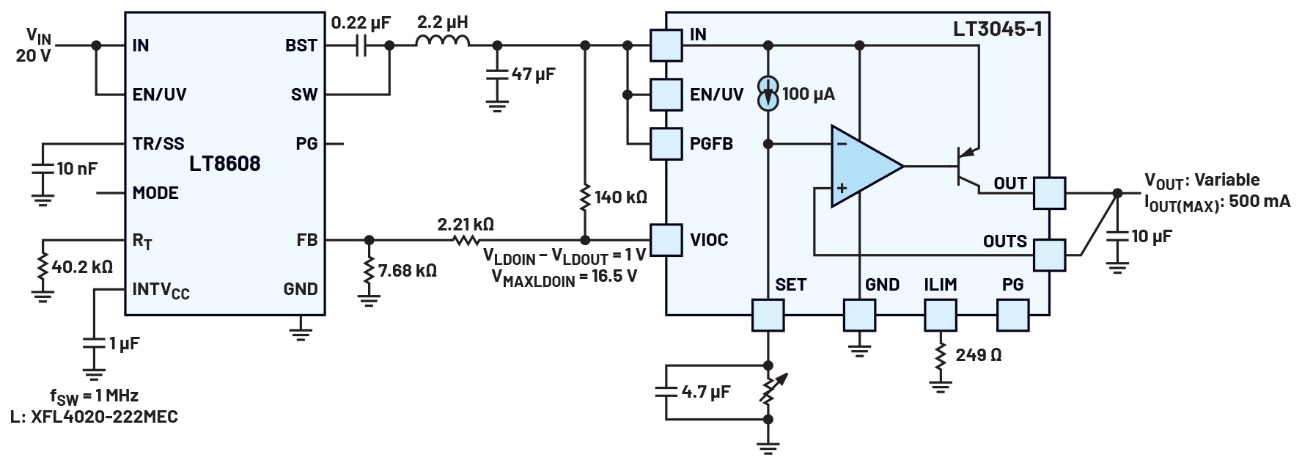
Figure 9. Typical LT3045-1 postregulating application.
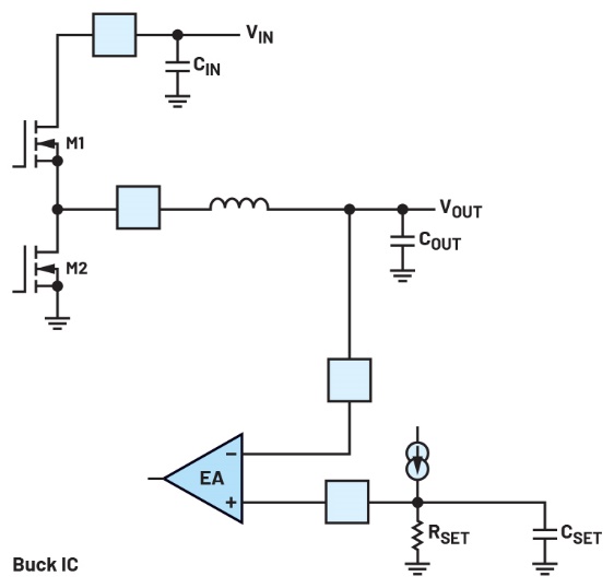
Figure 10. Current source reference architecture of a buck IC.
ADI utilizes a current reference architecture in several of its linear regulators, such as the LT3080 and LT3045, to achieve high precision and low noise. The LT3080 is an adjustable 1.1 A low dropout regulator designed with a precision current source and voltage follower, enabling it to support applications that demand high current and output adjustability down to 0 V. Highly integrated switching converters such as the LTM4653—a 58 V, 4 A step-down µModule® regulator—and those based on SS3 technology incorporate current reference architecture to enhance low noise performance and reduce EMI while maintaining high efficiency and small solution size.
The current reference architecture benefits are as follows:
- It enables output regulation to 0 V, which is hard to achieve using the traditional voltage reference.
- It simplifies output voltage setting by using a single resistor instead of two resistors from the traditional voltage reference. It saves component count and space.
- Consistent performance across the output voltage range since it operates at unity gain, ensuring stable bandwidth and transient response regardless of output voltage.
With ADI’s advanced SS3 technology, the output noise (0.1 Hz to 100 kHz) remains consistently low across the entire output voltage range, ensuring stable performance regardless of the output voltage level.
Normally, LDOs with VIOC capability are not designed to be paired with SS3 switching regulators because SS3 regulators don’t have the conventional FB pin. Figure 11 shows a new architecture where a current source reference switching regulator is used to generate an output voltage based on the resistor between the switcher SET pin and the LDO output.
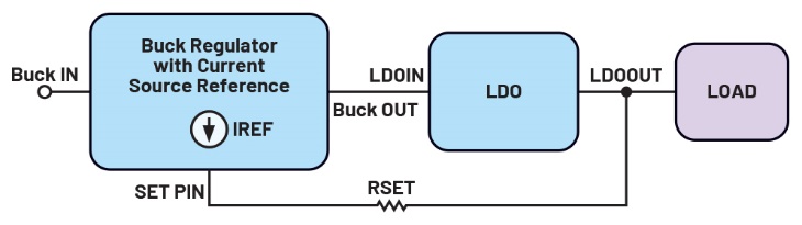
Figure 11. A block diagram of a buck regulator with current source reference and LDO for headroom control.
By utilizing DC-to-DC converters with current source reference features, a function that is similar to the VIOC feature of advanced LDOs can be implemented in a clever and efficient manner. In this setup, the first stage switching converter uses the current source reference at its SET pin and connects it through a resistor to the output voltage of the second-stage LDO, enabling dynamic headroom control and improved noise performance.
Conclusion
Switching regulator noise can affect analog signal chain components in different ways, depending on what frequencies each component is most sensitive to. Various filtering techniques can be applied, tailored to the specific frequency ranges the system aims to attain. Using an LDO is another effective approach, but it requires careful consideration of the trade-offs between PSRR and voltage headroom, which dictates the component efficiency, especially under dynamic output voltage or varying load conditions.
Part 2 will focus on optimizing LDO headroom control through current-referenced DC-to-DC converter design. It will cover practical implementations, circuit simulations, and performance evaluations—highlighting key considerations for noise-sensitive applications.
References
- Aldrick Limjoco and Jefferson Eco. “Ferrite Bead Demystified.” Analog Dialogue, Vol. 50, February 2016.
- Glenn Morita. “Understand Low-Dropout Regulator (LDO) Concepts to Achieve Optimal Designs.” Analog Dialogue, Vol. 48, December 2014.
- Yu Lu and Hugh Yu. “Low Noise Silent Switcher μModule and LDO Regulators Help Improve Ultrasound Noise and Image Quality.” Analog Dialogue, Vol. 56, April 2022.
Kyosuke Shimo joined Analog Devices Japan in 2022 as a new graduate and currently serves as a field applications engineer in the Industrial Customer Solutions Group. He supports power products and works closely with customers to address technical challenges and deliver innovative solutions. Kyosuke studied electrical and electronic engineering at the Tokyo Metropolitan College of Industrial Technology (KOSEN) and earned his master’s degree from Tokyo Metropolitan University in 2022. He believes “SPICE“ is the key—whether in circuits or in curry.
Ino Lorenz Ardiente currently serves as a power architect engineer under the Power Solutions Group at Analog Devices Philippines. He holds a bachelor’s degree in electronic engineering from Pamantasan ng Lungsod ng Maynila and a postgraduate diploma major in power electronics from Mapua University. He has more than 6 years of experience in the design, testing, and evaluation of high-power AC-to-DC and DC-to-DC converters before joining ADI in 2025.
Aldrick S. Limjoco currently works as a senior manager, power architect under the Power Solutions Group at Analog Devices Philippines. Since joining ADI in 2006, he has taken on diverse engineering roles focused on power management, including design evaluation, product applications, and applications research. Aldrick currently holds three U.S. patents and has authored/co-authored technical publications on the topics of switching regulator output ripple measurement techniques, novel techniques for low ripple power supply applications and ferrite bead intricacies. He earned his master’s degree in engineering (M.Eng.) from the University of Limerick in Ireland and his bachelor’s degree in electronics engineering from De La Salle University in Manila, Philippines.

Kyosuke Shimo joined Analog Devices Japan in 2022 as a new graduate and currently serves as a field applications engineer in the Industrial Customer Solutions Group. He supports power products and works closely with customers to address technical challenges and deliver innovative solutions. Kyosuke studied electrical and electronic engineering at the Tokyo Metropolitan College of Industrial Technology (KOSEN) and earned his master’s degree from Tokyo Metropolitan University in 2022.
Ino Lorenz Ardiente currently serves as a power architect engineer under the Power Solutions Group at Analog Devices Philippines. He holds a bachelor’s degree in electronic engineering from Pamantasan ng Lungsod ng Maynila and a postgraduate diploma major in power electronics from Mapua University. He has more than 6 years of experience in the design, testing, and evaluation of high-power AC-to-DC and DC-to-DC converters before joining ADI in 2025.
Aldrick S. Limjoco currently works as a senior manager, power architect under the Power Solutions Group at Analog Devices Philippines. Since joining ADI in 2006, he has taken on diverse engineering roles focused on power management, including design evaluation, product applications, and applications research. Aldrick currently holds three U.S. patents and has authored/co-authored technical publications on the topics of switching regulator output ripple measurement techniques, & novel techniques.