Power Delivery Network (PDN) for High-Speed PCB Design
March 04, 2022
Blog
The even distribution of various power and ground nets to various devices onboard is required for a good power delivery network design. It is desirable to have a dedicated power plane for every needed voltage.
The total number of such nets usually exceeds the available layers in the printed circuit board stack up. To alleviate this difficulty, designers frequently separate the planes so that numerous power or ground nets may be routed onto a single signal plane layer. While the split plane distributes various power and ground nets well, it also introduces an extra barrier to the signal return pathway. As a result, split plane designers must ensure that all power and ground nets are distributed evenly while maintaining the clear return paths required for sensitive high-speed signals. This ensures that the board is always operational, meeting the PDN requirements.
Introduction
In the early days of Printed Circuit Board (PCB) design, Power Delivery Network (PDN) was not a prominent consideration. With a high-speed design prevalent in the present context, PDN performance should be anticipated early in the PCB design and tailored to satisfy the device specification with lower voltage, higher current, and tighter noise margins. The objective of a PDN is to supply a clean and stable voltage to the core devices in a complex product design.
However, because of the parasitic added by the elements that make up the power network, the PDN analysis isn't perfect. It can be used to gauge and mitigate issues in major power rails at the early stages of the design. The PDN behavior is estimated by measuring the PCB level parameters such as the overall respective net impedance, DC resistance, and total loop inductance. To achieve reliable power delivery and low power loss, all PCB designs must have a PDN impedance of near zero.
Power rails on a PCB are part of the structure of the PDN. So, a transient generated on any one load may directly affect the rail and other loads might be impacted from that. The loading of the primary Voltage Regulator Module (VRM) is shown in Figure 1. Switching at Load 1 causes a transient voltage disturbance that is replicated by other loads. In this situation, components draw a large amount of current from the respective power rail with regards to the switching event. During this large amount of current draw, it interacts with the PCB parasitic all over the plane.
Many logic circuits switch at the same time in a practical integrated circuit, resulting in a complicated combination waveform as measured on the power rail.

Figure 1: PCB Transient effect on loads
Need of a Better PDN
Active components of a PCB require energy from the power supply to operate and a good PDN suffices this need. On a PCB, earlier, integrated circuit devices used to have just one power and ground pin that could be readily linked to a long trace. As circuit density increased, connecting circuits to power and ground planes on a multi-layer board became more challenging. As pin counts rose and IC power needs got more sophisticated, circuit boards began to face some of the following issues:
Electromagnetic Interference (EMI): The electronic circuitry got increasingly susceptible to EMI from both internal and external sources as its operating speed increased. Tuning the power and ground planes helps protect incoming and outgoing interferences to avoid EMI issues.
Ground bounce: Simultaneous switching noise, also known as ground bounce, occurs when a large number of digital signals transition states at the same time. It is observed that in data and memory buses if signals do not return to their respective reference ground plane due to fast switching, they observe a bounce effect. This impact might cause unwanted noise in the circuits that could lead to mistaken switching causing the device to malfunction. When the current is pulled into the PDN, the most typical transient voltage effect is ground bounce. When this happens, the ground reference plane voltage rises while the positive rail on the PDN remains constant. The reference ground level may be controlled with the aid of a well-designed PDN.
Power ripples: When a transient current propagates voltage fluctuation on the positive rail, it creates noise, or ripples, in the circuitry. These are not the same as the rectified AC output signal. These waves can cause crosstalk in other circuitry that can degrade the signal quality in those circuits. The current flow route and the parasitic items present in the current's route separate the two effects. Figure 2 shows the typical use case for ground bounce and power rail ripple.

Figure 2: Ground Bounce and Power Ripples
An Integrated Circuit (IC) has many more power and ground connections to handle, in addition to the faster switching speeds of current circuits. On a large processor chip with Ball-Grid Array (BGA) packaging, there are hundreds of power and ground pins with varying reference values. To power the processor, these pins might also consume a lot of current. As a result, ensuring that the power is free of spikes, ripples, and noise necessitates a well-designed PDN.
PDN Basics
The PDN can be represented as an R-L-C network and like any circuitry with some reactance, it can show a transient response that represents damped oscillation. The PDN impedance (Z) can be represented by a combination of resistance, inductance, and capacitance (R-L-C).
- Inductor: Z = jωL
- Capacitor: Z = 1/(jωC)
- Resistor: Z = R

Figure 3: RLC component for PCB PDN
Figure 3 shows the RLC components of a PCB PDN. The complexity of the die structures (field-effect transistor (FET) devices, diffusions, and so on) can be combined with the complexity of the package structures (vias, power planes, balls, and so on) and represented by simple series and parallel circuits for resonance purposes. The RLC circuits are in series from the perspective of component measurement (looking in from the outside). However, because the PCB PDN has a very low impedance, the On-Die Capacitance (ODC) is in parallel with the packaging inductance from the inside looking out (looking out from the inside). When the same circuit components are put in series and in parallel, they behave differently. The frequency response of a typical series and parallel RLC circuit is shown in Figure 4.

Figure 4: Frequency response for series and parallel RLC
Now, copper traces for power pins and copper planes for ground pins also play a crucial role in PDN performance. A simplified model of PDN can be shown in figure 5.

Figure 5: A simplified PDN model
PDN is like a multiport network. The switching component on DC buses can impact the overall DC buses’ power distribution. It can cause some variations in the DC power sensed by all components on the PDN. In simulations, Z-parameters are used to benchmark the relationship between impedances seen at various ports. The voltage fluctuation visible at a PDN port in relation to the current drawn into all PDN ports is defined by this parameter matrix.
The target/maximum allowable impedance (PDN) puts a limit on the peak allowable impedance value for the PDN. The waveform of transient ripple on the power lines is determined by the PDN impedance that converts to jitters for a high-speed IC. For switching the IC, it draws current from the power buses that represent the pulse waveform via the PDN. Any capacitors and/or parasitic capacitances in the PDN will offer some reactance, resulting in a transient response in the PDN. The purpose of the PDN impedance control is to minimize the effect of any transient waveform.

Figure 6: PDN impedance target
The goal is to keep the target spectrum below the target impedance value, from DC to the target frequency. The Frequency Domain method is used for Target Impedance calculation. Due to the predominance of the parasitic planar spreading inductance and package inductances, adding a reasonable number of decoupling capacitors does not lower the power rail impedance |ZEFF| below the target impedance (ZTARGET).

For example - to effectively decouple 0.9 V rail, FTARGET of 50 MHz, 5% ripple (AC Component), and maximum allowable current of 4A (considering 50% as transient current) ZTARGET can be estimated as:

The PDN utilizes PCB discrete capacitors (decoupling), interplane capacitance, and inductance to provide a very low impedance profile (Zeff) below the target impedance (ZTARGET) up to the desired frequency.
The voltage variations on the power bus are caused by a high PDN impedance. The best method is to reduce the PDN impedance to the lowest level achievable. This is accomplished by carefully selecting decoupling capacitors and strategically arranging neighboring power or ground planes to achieve high interplane capacitance.
The PDN impedance and transient current determine the amount of transient waveform of ripple on the PDN bus. As impedance can be characterized as the functional domain of frequency, the impedance curve must be below the set target/peak value over the respective signal bandwidth. This relationship can be derived from Ohm’s law. Figure 7 shows a typical curve for impedance with respect to frequency.

Figure 7: A typical impedance vs frequency curve
PDN Analysis
To extract PDN performances of the PCB layout, one may need the following as inputs:
- Design Schematic
- PCB Stack-up with dielectric properties (Dk and Df)
- PCB Layout
- S-parameters capacitors models from the manufacturer
- Power Integrity tool
PDN impedance can be impacted by various factors, including PCB structure and PCB parasitics in the elements of a circuit. This can be further evaluated from two perspectives - circuit simulators and field solvers.
A. EM-Field Solver method
A field solver sets boundary conditions on the electromagnetic field instead of circuit characteristics and directly solves Maxwell's equation. It is feasible to construct the Z-parameter matrix for the PDN structure and estimate the impedance of a potential multi-port PDN using these results. PDN impedance can be represented as an impedance matrix with Z-parameters:

Figure 8: Impedance Matrix
For an N-port network, PDN impedance can be defined in terms of a Z-parameter matrix. Diagonal terms represent self-impedance and off-diagonal terms represent transfer impedance. Transfer impedance explains how current drawn into one port causes a voltage disturbance to all other ports in the PDN, whereas self-impedance or characteristic impedance quantifies the power disturbance experienced at a port in a PDN due to the current drawn into the same port.
To solve this and calculate the PDN impedance matrix shown above, apply a 3D electromagnetic field solver tool that accepts data straight from the PCB layout. This simulation method is the quickest for calculating the PDN impedances with several power buses and their branches, but it is time-consuming for designing decoupling networks for the PDN.
B. Circuit Simulations
Circuit simulations cannot account for all parasitics in a PDN impedance calculation due to the complex structure of the actual PDN unless they are put as comparable circuit components. However, a series of decoupling capacitors attached to the PDN to give consistent DC voltage can be used to imitate the impedance spectrum. One may execute parameter sweeps on a capacitor network that contains parasitic inductances in the capacitor models using a SPICE simulation engine within schematic design tools. The purpose is to experiment with different capacitor values and numbers to find the ideal capacitor configuration that minimizes the PDN impedance.
The first step in assessing and regulating the PDN impedance is to use circuit simulation. Because, impedance fluctuates with frequency, calculating the impedance spectrum from DC to a very high frequency is your aim in controlling the PDN impedance. The PDN impedance should be sufficient to cover the signal bandwidth required by your components. In a circuit simulation, this necessitates considering the following factors:
Capacitor self-resonance: Because of their Equivalent Series Resistance (ESR) and Equivalent Series Inductance (ESI), decoupling or bypass capacitors on every component have some self-resonance frequency. Datasheets can be used to obtain typical values for the self-resonant frequency of selected capacitors.
Interplane capacitance: The capacitance between the ground and power planes of your PDN is determined by the stack-up of PCB. It is necessary to verify that PDN in a high-speed design PCB has appropriate decoupling ─ this is a parasitic effect. It is possible to minimize the dependency on discrete decoupling/bypass capacitors by taking advantage of the inherent capacitance in a stack up. For a standard thickness 6-layer PCB, typical values are 0.5 pF/sq. mm.
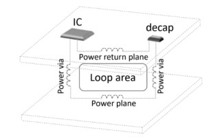
It's essential to remember that there are certain things that a circuit simulation can't evaluate. Parasitics in capacitors like ESL and ESR should be considered. Interplane capacitance and other parasitics cannot be explicitly accounted for. Instead, account for any parasitics in the design as equivalent circuit parts. This necessitates estimating the plane capacitance and the plane loop inductance. Figure 9 depicts the formation of a typical loop inductance.

Figure 9: Loop inductance Image
The PDN behavior in each frequency can be resistive, inductive, or capacitive. It is a combination of series and parallel resonances. A typical spice simulation graph is represented in Figure 10.

Figure 10: Spice Simulation
Some of the industry-standard tools for doing analysis are DC drop analysis, AC decoupling analysis, Power Integrity and PDN optimization HyperLynx, PDN Analyzer, PDN Tool, and Allegro Sigrity. Some online tools used for impedance calculation are CircuitLab and PDN Tool.
PCB Design Guidelines For PDN
Achieving PDN target impedance can be arduous. Using the guidelines mentioned below, you can achieve a PDN close to the target value.
- Always adapt symmetrical layer stack up (i.e., the top layers must be mirrored in bottom layers). The combination of an uneven layer stack up and high heat and pressures of the manufacturing process might cause the board to distort.
- Prepreg and core layers are symmetrical in their thickness (throughout the stack up).
- Assign power and ground layers first and as close as possible i.e., minimum dielectric thickness between power and ground planes.
- If possible, keep the power and ground plane layers in the board layer stack symmetrical to maintain signal integrity.
- Try to maintain the highest density copper layers in the middle of the stack. This must, once again, be done in combination with proper signal integrity procedures.
- For different plane layers, use the same copper weight. Consider using metal fillers (copper pours) in places where there isn't a lot of metal.
- Most essential, before committing to suggested board layer stack up, verify with PCB manufacturer to guarantee that process can fabricate it.
- Confirm with the fabricator the minimum Anti-pad (the void area around a via on internal plane layer) gap that he can do reliably. Follow the same in the design as it helps lower the DC resistance.
- PCB floor planning should be given the highest priority and shall be considered and worked upon while schematic is 50-60% done. You can speed up the process by leveraging the reference design right from the start.
- Use decoupling capacitors after major component placement. Inductance is an enemy here and capacitance is a lifesaver. The higher the number of capacitors the lesser number of failures in the PDN.
- Select a variety of capacitor values so their resulting impedance profile is flat and looks resistive all the way to the frequency.
- Via on pad should be followed wherever possible in the design. Not only for BGA fanout but for discrete also. Avoid via sharing, it could be disastrous.
- Placement and orientation of decaps could be optimized using a mix of topside or backside capacitor placement.
- Do not share power trace for net critical to noise –check design guidelines and layout checklist respective to the device.
- Larger power loop increases inductance in the path, avoid creating loop inductance paths.
- Use as many parallel return paths in the power-ground interconnects.
- Each power rail pin should have decaps. Connect them with the through-hole via if on the other side of the board.
- Connect the same nets with vias. Blind and buried via should be staggered.
- Copper planes can be used for thermal improvement.
- Make small islands for power rails, if not possible then wider traces should be followed depending upon the estimated current requirement.
- Fanout strategy must be planned to minimize the return path and thus the loop inductance.
- Place the through-hole vias on the four corners of the IC to provide an easy return path.
- To reduce the voltage response to a transient current step, increase the capacitance or decrease the inductance.
Conclusion
Meeting PDN impedance specifications ensures minimal or close to zero chance of failure due to PDN issues for all devices under all operating conditions. Failure to meet the PCB Z specifications does not mean that every device will experience a failure. It means that for mass production, quantities operated over the valid range of voltages and temperatures allowed by the device specification, the probability of failure of some percentage of the devices is not zero.
Regardless of the topology, one should aim to design for the lowest feasible PDN impedance within the desired bandwidth using the design guidelines. The PDN impedance will never be zero, although it is predicted to reach milliOhm values at GHz frequencies. The use of many decoupling capacitors with varying ESL values and adjacent planes aids to maintain low PDN impedance, which limits power bus voltage swings and jitters on output signals to a minimum. With many design criteria that go into producing a successful PDN, having robust design rules and constraint management systems are also beneficial.
eInfochips, an Arrow company, has a strong ecosystem of manufacturing partners who can help, from electronic prototype design, manufacturing, production, and certification. eInfochips is a leading global provider of product engineering and semiconductor design services. For more information on our PCB design solutions, please connect with our experts.
Priyesh Pandya is a product manager involved in the development and deployment of high-speed solutions for the past 15 years. He works to improve customer design processes and solve complex technical challenges associated with high-speed signal transmission and EMI emissions.
Bhavesh Jaiswal is senior engineer and involved in development of various high-speed boards. He is insightful in overcoming challenges in product development lifecycle.
References
- L. D. Smith, R. E. Anderson, D. W. Forehand, T. J. Pelc, T. Roy, "Power Distribution System Design Methodology and Capacitor Selection for Modern CMOS Technology," IEEE Transactions on Advanced Packaging, Vol.22, No.3, P284, August 1999.
- E. Bogatin, L. D. Smith, “Principles of Power Integrity for PDN Design--Simplified: Robust and Cost Effective Design for High Speed Digital Products”, Pearson, 2017.
- Power Delivery Network Analysis, TI Application report. SWPA222A – November 2012.
- Ztarget calculation and usage for PDN Simulation, Article 76050, Xilinx, 2021.
- PCB Power Integrity Analysis, https://www.cadence.com/en_US/home/tools/pcb-design-and-analysis/pc-design-flows/power-delivery-network-pdn.html
- Cadence Allegro Sigrity PI solution, https://www.cadence.com/en_US/home/tools/pcb-design-and-analysis/si-pi-analysis/sigrity-aurora.html
- Hyprelynx, https://eda.sw.siemens.com/en-US/pcb/hyperlynx/
- PDN analyzer, https://www.altium.com/pdn-analyzer
- PDN Tool, https://www.intel.com/content/www/us/en/support/programmable/support-resources/signal-power-integrity/power-distribution-network.html
- Free Impedance Analyzer on your Desktop, https://www.signalintegrityjournal.com/
- PDN Tool V1, http://app.pdntool.com/
- Circuit simulation and schematics, https://www.circuitlab.com/
- Power integrity, https://en.wikipedia.org/wiki/Power_integrity

Priyesh Pandya is a product manager involved in the development and deployment of high-speed solutions for the past 15 years. He works to improve customer design processes and solve complex technical challenges associated with high-speed signal transmission and EMI emissions.
Bhavesh Jaiswal is senior engineer and involved in development of various high-speed boards. He is insightful in overcoming challenges in product development lifecycle.