Starting into the World of Small-Run PCBAs
April 12, 2021
Blog
A little over a year ago I ordered my first printed circuit board (PCB) from OSHPark, which contained an ATtiny85, along with resistors and a few blinking LEDs. Since then I’ve designed several more boards, and fairly recently I made the switch to surface mount components.
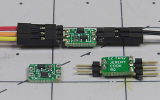
Along the way, I came up with a fan control board for the Raspberry Pi, which I decided to sell on Tindie. This little board started out as a through hole design, which morphed into something even smaller that uses surface mount components. As these parts were actually selling, I got a little tired of assembling every single one by hand.
The next logical step was to set up my design to be made by someone else as a PCB assembly, commonly known as a PCBA. After a bit of research and experimentation, I’m happy to report that my order came out correctly, and I’ve sold a few of them since then.
There is something really satisfying about providing a product to others that you’ve designed, and having them made off-site means that you can sell as many as you want. So, how exactly do you take this final step towards automation?
KiCad PCBA With PCBWay
So far, I’ve used KiCad for all of my PCB designs, and in this case, I used PCBWay to make and assemble the boards. So, while the concepts in this article should be broadly applicable, the specifics are largely for PCBWay and KiCad’s PCB Layout Editor. Once you have your Gerber (PCB fabrication) files set up, the next steps are to generate a centroid file, which outlines where the components will be placed, as well as a BOM (bill of materials), which specifies the components to be used.
Centroid File, AKA Footprint Position
The procedure for PCBWay is outlined here, starting with setting the Drill and Place Offset, as well as the Layer Alignment Target in the Place dropdown. Note that the terminology in that link is slightly different than what I have here per my usage. I would guess is due to the version of KiCad that I’m using (5.1.6-0-10_14) versus what was used when those directions were generated.

Next, click on File > Fabrication Outputs > Footprint Position (.pos) File, and use the settings shown below. This will generate a text file that you can open up with a text editor.

After experimenting with the offset/target, and looking at what I submitted, it appears I didn’t actually set the offset/target properly. While PCBWay apparently figured out what I meant, the X/Y positions in the text file had offsets much larger than the board. Best set things up properly to avoid any confusion.
Bill of Materials, BOM
To generate a basic BOM, go to File > Fabrication Outputs > BOM File, and save it. You’ll get a comma-separated values (CSV) file, which can be opened as a spreadsheet. This will generate basic info about the parts designator and package, which corresponds to info on the position file. In other words, this tells the manufacturer what to place, while the position file explains where to place it.

To get into what specific parts you need, in the proper format, I used PCBWay’s template, found here. This involved taking the spreadsheet generated by Kicad, and modifying it to fit the template, adding specific info about the parts I wanted to use, such as manufacturer, part number, and other notes. In retrospect, the best way would likely be to past into the PCBWay template from the Kicad file, but it looks like I did it the other way around. Other manufactures should have similar templates, and there’s a script available to get things in the proper format you decide to go with JLCPCB, though I haven’t tried it.
After I uploaded my files, they sent a spreadsheet back to me, which included part substitutions for my approval, which I gave. I was also informed that they’d be panelizing my boards (I ordered 20) for easier assembly. After assembly, they took care of separating each one, and actually placed them into their own individual bags, so the process was mostly transparent to me.
Manufacture, Assemble, Ship!

(Assembled together on a panel before separating and shipping - Image Credit: PCBWay)
With my approval on March 11th, they got to work building my boards, and shipped it on March 29th, 18 days later. From there, it was a quick trip via DHL, arriving the morning of April 1st. So 21 days from order approval, to an entirely custom PCB assembly arriving at my doorstep in Florida from China. Really incredible.

(Boards were perhaps lonely, but well protected in their own individual bags - Image Credit: PCBWay)
Not too long after, I got another order on Tindie, soldered headers on (available as an option), and shipped it on April 5th. So, with a bit of quick design work, it’s possible to go from idea, to design, to actually selling a custom manufactured device–sourced from halfway around the world–in under a month. Considering the technology and logistics involved, plus the fact that I paid well under $100 for the service, it’s absolutely mind-blowing.