Improving DDR performance by switching from wirebond to flip chip
October 01, 2012

Flip chip chip-to-package interconnects are turning next-generation DDR interface technology upside down.
The DDR interface transfers data at both the rising and falling edges of the clock signal. This technique has been used as a communication link for DDR Synchronous Dynamic Random-Access Memory (SDRAM), microprocessor front-side buses, Ultra3 Small Computer System Interface (SCSI), and accelerated graphics port buses. In each cycle, data is sampled at the rising and falling edges of the clock, and the maximum data frequency is typically twice the clock frequency.
The trend in DDR technology is toward higher data rates and lower voltage levels. For a system to function accurately, its signal integrity performance must be optimized and meet certain minimum requirements. Although the DDR2/DDR3 interfaces are not as fast as a Serial Link interface, signal integrity issues are significantly more challenging and will become an even bigger problem with DDR4. This is due to the parallel versus serial nature of these interfaces. Signal integrity concerns such as crosstalk and power supply noise are dominant for parallel interfaces and steadily get worse as data rates increase.
With the industry shifting toward DDR3 and higher data rates, the data valid window or Unit Interval (UI) during which data can be reliably sampled steadily shrinks, and sensitivity to signal integrity issues dramatically increases. The package becomes an important consideration at these high data rates, especially with respect to the chip interconnect method. The current IDT DDR3 package is configured as a wirebond die. The following discussion will highlight the benefits of changing the DDR3 die to a flip chip type and showcase the resultant performance benefits.
DDR interface challenges
First-generation DDR interfaces were designed to send and receive data at a maximum data rate of 400 Mtps with a respective bit period or UI of 2.5 ns. These interfaces typically used a 2.5 V power supply. Current DDR3 interfaces run at 1,600 Mtps, and DDR4-based systems are expected to run at 3,200 Mtps. At that data rate, each UI is only about 312.5 ps, with the power supply dropping to 1.2 V.
This evolution in DDR technology introduces several challenges to physical interconnect design:
- Shrinking bit period: A shorter bit period results in a shorter setup and hold time frame, making it extremely difficult to meet timing between clock and data signals.
- Fast signal edges: To accommodate shrinking bit periods, signal edges are increasingly getting sharper, exacerbating crosstalk and power supply noise performance concerns.
- Lower voltage levels: For a 2.5 V supply, a 5 percent noise tolerance results in a maximum acceptable level of noise of 125 mV across the chip power and ground nodes. That same 5 percent noise tolerance for a 1.2 V supply translates into just 60 mV of acceptable noise across the same power and ground nodes. Interconnect design and selection becomes a critical component to meet these tight noise tolerances.
The package forms a critical component of the total system interconnect, and a suboptimal package interconnect selection can significantly degrade device performance. The current IDT DDR3 device uses wirebonds as a means of connecting the chip to the package substrate. The 3D nature of the wirebonds makes controlling the electromagnetic fields emanating from aggressor signals extremely difficult to manage. Wirebonds, in general, are inductive in nature, and the mutual inductance between two neighboring wires is a major contributor of signal-to-signal crosstalk. The inductive wirebonds also cause power supply impedance to increase with a resultant increase in power supply noise at the chip.
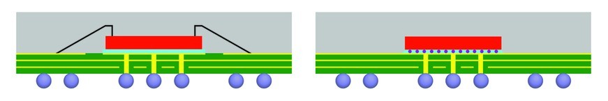
Removing these wirebonds and converting the chip-to-package interconnect to the flip chip will eliminate a key source of signal integrity concerns without affecting the overall package form factor. Figure 1 shows a cross- section of the two chip-to-package interconnect types with all other features being equal.
|
|
Understanding crosstalk
Crosstalk is caused by the leakage of electromagnetic signal energy from one conductor to another through mutual capacitance (electric field coupling) and mutual inductance (magnetic field coupling).
Capacitive crosstalk
In a victim-aggressor situation, capacitive crosstalk injects current from the aggressor line onto the victim line with the magnitude of crosstalk proportional to the rate of change of voltage and the amount of mutual capacitance between the two lines. The injected energy will split and flow toward both ends of the victim line – both ends being near end (close to the driver side) and far end (close to the receiver side).
Inductive crosstalk
Crosstalk due to mutual inductive coupling induces voltage on the victim line proportional to the rate of change of current on the driven line and the magnitude of mutual inductance between the two conductors. The current due to the induced voltage flows in the opposite direction of the driven line from the far end to the near end (based on Lenz’s law).
In substrate-based packages, crosstalk can be divided into crosstalk in the transmission line section of the package interconnect and crosstalk in the 3D structures of the package interconnects such as vias, wirebonds, and solder balls. In the transmission line section of the package structure, crosstalk is predominantly electromagnetic, while in the 3D section it is mostly inductive. For most packaging applications, far-end crosstalk is almost always negative, identifying inductive crosstalk emanating from the 3D sections of the package as the dominant crosstalk mechanism. With the wirebonds eliminated (mutual inductance reduced), the flip chip version of the package shows much less far-end crosstalk than the wirebond version, as shown in Figure 2.
|
|

Crosstalk effects on modal delays
The flight time of a signal through a conductor depends on how the neighboring coupled conductors switch. This difference in flight time is exacerbated as crosstalk between conductors increases. In a multiconductor system, there are three possible switching modes: quiet mode, odd mode, and even mode:
- Quiet mode: If the rise and fall times of the victim signal do not coincide with the neighboring coupled aggressors, or if the victim signal is held quiet, this switching mode is called quiet mode.
- Odd mode: If the rise and fall times of the neighboring coupled aggressors coincide with the victim signal, and if the aggressors are switching 180° out of phase with the switching signal, this switching mode is called odd mode.
- Even mode: When the neighboring aggressors’ switch is in the same phase as the victim signal and at the same time, this switching mode is referred to as even mode.
In a coupled system, a signal experiencing odd mode switching always arrives earliest at the receiver, followed by the signal in the quiet mode and lastly the signal experiencing even mode. This spread in the signal flight time between switching signals in an I/O bank increases as crosstalk increases. In a DDR-type system where a common clock is used to sample multiple, parallel signal bits, this spread in crosstalk-induced skew can have a detrimental impact on the setup and hold time window available for proper clocking. And as the data rate increases with the associated shrinkage in UI, reducing crosstalk to improve setup/hold time windows will become paramount.
Figure 3 compares the modal delay spreads of the two package types. Wirebond delay is more spread out, with the total modal delay spread of 41 ps compared to just 15 ps for the flip chip variation. With the UI for DDR4 applications expected to be half of DDR3, this increase in package skew for wirebond packages will make timing extremely challenging to meet, and hence flip chip will be the preferred interconnect option.
|
|

Power delivery to the chip
Efficiently delivering power to the chip requires reducing the input impedance of the power delivery network looking out from the chip power and ground nodes. The package type and chip-to-package substrate interconnect technology are critical components of the overall system power delivery network. Package impedance is largely a function of the loop area formed by the power and ground interconnects and the type of chip-to-package interconnect method used. Eliminating wirebonds from this loop reduces loop inductance and hence the impedance by more than 50 percent, with a resultant drop in power supply noise at the chip. The magnitude of noise reduction will be a requirement for optimal DDR4 interface performance.
As the adoption of DDR4 will require tighter noise and timing budgets, flip chip will become the technology of choice for chip-to-package interconnects. Inherently inductive wirebonds will affect crosstalk, timing, and power supply noise performance at these high data rates. By providing key advantages over wirebond interconnects, flip chip dramatically improves important performance metrics for DDR interfaces.
Integrated Device Technology [email protected] www.idt.com
Follow: Twitter Facebook Google+ LinkedIn YouTube