Printed electronics embed intelligence - Everywhere
March 01, 2015

To date, this proliferation of intelligent sensing has been hampered by the cost, weight, size, form factor, and power consumption of electronic syste...
To date, this proliferation of intelligent sensing has been hampered by the cost, weight, size, form factor, and power consumption of electronic system components and boards that are manufactured using conventional techniques. However, new advances in printed electronics have extended the sensing and data capture reach of embedded systems far beyond what we have known, while also incorporating much-needed security features. Coupled with the development of smart algorithms that emphasize the use of small data sets to make presentation and analysis of acquired data more efficient and actionable, the promise of the IoT paradigm shift in embedded computing is primed for fulfillment.
So far industry has done admirably leveraging highly integrated, PC board-based embedded systems and low-power techniques to reduce the cost and improve the efficiency of IoT systems. Now we have reached a critical juncture in that the next level of actionable intelligence in the IoT requires scaling intelligent sensory inputs from tens, hundreds, or thousands of nodes to millions or even billions. Though numbers vary, IDC predicts an installed base of over 28 billion endpoints by 2020, all of which need to maintain an acceptable level of cost, efficiency, and security. As the reach of affordable electronic intelligence further expands to include high-volume consumer goods, the number of connected objects could easily reach the trillion units predicted by IBM.
As the number of forecasted endpoints rises, the pressure has shifted to algorithm developers to find ways of filtering the type and amount of data collected in order to reduce the amount of time and processing power required to gather usable information (Figure 1). This has led to much research in data stream analysis, which, for example, prescribes that instead of sensors constantly reporting their states and creating terabytes of data to be processed and stored, algorithms are used that set predetermined pressure and temperature ranges so that alerts are only sent when these limits are surpassed. As a result, network and system processing, as well as storage overhead, can be reduced, improving overall efficiency [1,2].
|
|

This focus on smaller data sets, combined with the opportunity for sensing nodes to penetrate new applications and markets – such as labels, disposable healthcare, pharmaceuticals, consumer goods, supply chain, and product security – has created a pull for innovative manufacturing and sensing technologies like printed electronics. Using such techniques with a flexible, low-power processing solution can help designers add intelligence to their embedded systems, both wired and wirelessly, at low cost.
The new foundations of printable electronics
Printed electronics have evolved substantially from the early implementations of basic conductive copper or silver traces printed on hard (and later flexible) substrates to which conventional electronic components were attached. Now, thanks to advances in materials science, printed electronics incorporates a wide variety of capabilities, from roll-to-roll memories to printable thin film transistor (TFT) logic and even wireless communications.
One recently commercialized core building block in printed electronics is printed memory. The printed memory works on the principle that when a voltage is applied to a ferroelectric polymer material the dipoles within the polymer layer align in one of two directions, depending on whether the voltage is applied to the top or bottom electrode. When voltage is removed, the material remains in the same state and can be read as a one or a zero, making it equivalent to a non-volatile memory (NVM) cell, but at lower cost and available in a thin, flexible self-adhesive label (Figure 2).
|
|

But while memory has many applications, printed systems also require logic. There are at least two options here. First, a collaboration including Xerox Palo Alto Research Center (PARC) and Thin Film Electronics ASA resulted in printable TFT transistors. Second, a hybrid printed manufacturing process called printed dopant polysilicon (PDPS) has been developed to address RF and other applications that require high-performance transistors, which we’ll explore further.
The PDPS process, which enables NFC barcode and sensor-based NFC smart label products, enables the design of printable, high-frequency RF circuits for printed systems connected to smartphones using NFC. The addition of NFC capability has opened up a new spectrum of smartphone-centric applications, some of which are only just starting to take shape.
In Thin Film ASA’s Smart Label, memory, logic, and NFC are combined with a temperature sensor and low-profile batteries to warn of temperature deviations outside factory-set limits. While the flexible substrate allows it to adapt to curved surfaces, the sensor can be set with threshold detection as low as -2 °C and as high as +30 °C. The completely self-contained system requires no external power or wiring, with the underlying sensor platform serving as a base for other future sensing mechanisms, such as timing, humidity, or even blood oxygen counts (Figure 3).
|
|

IoT security assured
While printable electronics have the ability to penetrate deep into the IoT, designers need to be assured of the security features of the technology in order bring it to next-generation system designs.
In the case of printed memories, this assurance comes at three levels. Firstly, the basic makeup of ferroelectric materials in printed memory produces a distinct signature that can only come from a genuine part. Second, this characteristic signature can only be read through physical contact with a reader. Finally, the memory itself is not IP addressable, thereby preventing external intrusion.
In the case of NFC tags and smart labels, security is provided by the short-range readability of NFC tags (integrated read-only memories that cannot be electrically modified), and the fact that the NFC interface is also not IP addressable.
Development and getting connected
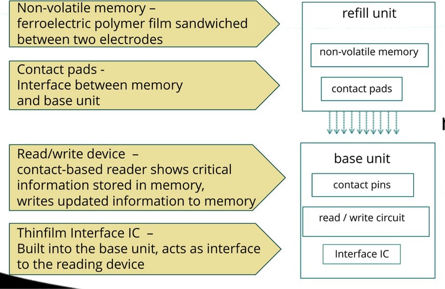
As with any new technology, getting started right is critical. Support must be in place to ensure a rapid and painless development process, so to streamline development with printed memories in "smart consumables" and brand protection applications designers can start with a basic kit comprising memory labels and a corresponding memory interface IC (in bare die or packaged form) that reads and writes to the printable memory (Figure 4). Code support is also available for integration with the host microcontroller.
|
|
For NFC-based applications, connecting a smart label or node to the cloud must be simple. Support here comes in the form of the EVRYTHNG Active Digital Identity platform.
EVRYTHNG handles the assigning of a unique digital identity to each physical product. The cloud-based Software-as-a-Service (SaaS) platform can connect and manage all types of intelligent items, from a connected washing machine to an NFC-enabled sensor label based on printed electronics. The EVRYTHNG engine manages a dynamic profile for each item and enables interactivity through a uniquely addressable API. This makes the product or device always accessible, manageable, and intelligent.
The printed electronics differentiator
Now, embedded developers are free to develop highly scalable systems that take advantage of the step increase in the number of IoT nodes by adding cost-effective, efficient technology to better service their end customers.
Thin Film Electronics ASA www.thinfilm.no @ThinfilmMemory linkedin.com/company/thin-film-electronics blog.thinfilm.no/
References:
[1] Data Streaming Algorithms for High-Quality Clustering
www.cis.upenn.edu/~sudipto/mypapers/stream_icde.pdf
[2] Mining Data Streams
infolab.stanford.edu/~ullman/mmds/ch4.pdf