Voltage Input-to-Output Control for Linear Regulators—Part 1: Quick Start and Benefits
November 03, 2025
Story
Part 1 of this two-part series introduces voltage input-to-output control (VIOC) systems that are commonly configured as a combination of low dropout (LDO) regulators with the VIOC feature and buck-topology switching regulators. The article then gives guidance for VIOC system design, including a list of suggested pairs of LDOs and switching regulators and the reasons for the pairing. Lastly, it shows how the use of the LDO’s VIOC feature can reduce noise at the LDO output, optimize power dissipation, protect the system during faults, and ensure proper operation during dynamic conditions like startup and overload. Part 2 expands on the guidance for VIOC system design from Part 1 and also discusses VIOC theory of operation and background.
Introduction
In the realm of power management, low dropout (LDO) regulators play a crucial role in ensuring high performance power delivery to electronic components. Low noise performance in LDOs is vital, especially in noise-sensitive applications like precision analog circuits, RF systems, and medical devices, where LDOs ensure clean power delivery, minimizing interference and enhancing signal integrity. When combined with voltage input-to-output control (VIOC) functionality and a compatible switching regulator to provide the LDO with power, LDOs can further enhance their performance by creating a system that consistently maintains an optimal input-to-output voltage for noise-minimizing, high power supply rejection ratio (PSRR), in addition to operation that is efficient, protected, and highly capable. This article delves into the intricacies of implementing VIOC, exploring its advantages and practical applications. By understanding the synergy of VIOC, engineers can optimize power management solutions for a wide range of electronic devices.
LDOs, with or without VIOC, are part of the power management product category. Power management includes integrated circuits (ICs) known as regulators or converters that supply power for electronic loads like amplifiers, data converters, or processors. LDOs are a subset of power management ICs, designed to directly power electronic loads, and are known for influencing load performance, minimizing unwanted interactions between loads, and ensuring proper sequencing (turn-on and turn-off) of power ICs and loads in a system.
An LDO with VIOC has internal circuitry that provides an external signal to control the output of the switching regulator that provides power to the LDO, typically to maintain a constant input-to-output voltage for the LDO as shown in Figure 1. Linear regulators are fundamentally transistor circuits that provide power with relatively low noise but are sensitive to their input-to-output voltage, which determines their efficiency. Switching regulators (or switchers) transfer energy by rapidly switching a power transistor (switch) on and off. The switching regulator uses the power switch along with an inductor and diode to efficiently convert its input voltage to a voltage that is more suited to power the LDO.
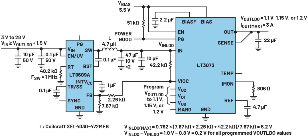
Figure 1. This VIOC system maintains a consistent input-to-output voltage for the LDO.
Using VIOC to Combine a Buck and an LDO for Enhanced Performance
A typical VIOC circuit consists of a buck switching regulator that provides power to an LDO with the VIOC feature. The resulting circuit is a powerful configuration that leverages the high efficiency of the buck regulator with the low noise performance of the LDO. A buck regulator, also known as a buck converter or step-down converter, is a type of switching converter that efficiently converts its input to a well-regulated output that is lower than the input voltage.
The first step to creating a VIOC circuit is to select the LDO and the switching regulator. Analog Devices offers several LDOs with integrated VIOC functionality. The LT3045-1 and LT3041 series and the LT3073, LT3074, and LT3078 series have the latest version of the VIOC feature. The LT3045-1 and LT3041 linear regulators have an output current range from 500 mA to 1 A and an input voltage that ranges from approximately 2 V to 20 V, while only requiring one input supply. The LT3073, LT3074, and LT3078 have an output current range from 3 A to 5 A and an input voltage that ranges from 0.6 V to 5.5 V, while requiring an additional low current BIAS input supply. Any switching regulator with a feedback (FB) pin can be combined with these LDOs using VIOC, but before choosing the design’s switching regulator, consider the following:
- VIOC-capable LDOs can be used with any type of switching regulator topology, but are most often used with buck regulators.
- The LT3045-1 and LT3041 LDOs must be paired with a switching regulator that has a FB voltage of 1 V or less so the LDO VIOC pin can operate at 1 V (see the data sheet for details).
- A switching regulator that has an available compensation pin may be easier to stabilize in a VIOC system than a switcher that does not.
- Switcher and LDO evaluation boards make it convenient to evaluate the operation of VIOC system hardware.
- LDOs with VIOC capability are not designed to be paired with Silent Switcher® 3 (SS3) switching regulators because SS3 regulators don’t have the conventional FB pin.
- µModule® regulators with an integrated top feedback resistor will not be able to maintain a consistent input-to-output voltage at the LDO, compared to typical VIOC circuits.
- A circuit that uses VIOC requires a dedicated voltage rail as the stage prior to the LDO, rather than a stage that supports many rails.
- VIOC requires more components compared to a standalone LDO design. The additional components required for a VIOC circuit are additional resistors in the feedback divider for the switching regulator that provides power to the LDO and usually additional capacitance for the switching regulator output.
To simplify the design process, ADI provides guidance on which buck switching regulators pair best with specific LDOs that have the VIOC feature. Table 1 lists the best switchers to combine with the recommended LDOs that have VIOC, along with descriptions of all the LDOs. These pairings are based on the considerations listed earlier, so follow the guidance given above and in Table 1 when making a VIOC circuit that consists of a buck regulator and an LDO with the VIOC feature. Reference designs of many VIOC circuits are provided in the data sheets of the LDOs listed in Table 1.
Table 2 provides descriptions of the buck regulators that are specified in Table 1. This information helps designers choose a regulator that not only meets electrical requirements but also aligns with constraints such as the switcher’s input voltage range, load current capability, and operating current. In addition to the recommended switching regulators for VIOC use, Table 2 includes the switcher’s feedback pin voltage, available modes, evaluation board part number, and compensation pin availability.
VIOC’s Noise-Minimizing, High PSRR Benefit
As mentioned, when combined with VIOC functionality and a compatible switching regulator to provide the LDO with power, LDOs can further enhance their performance by creating a system that consistently maintains an optimal input-to-output voltage for noise-minimizing, high PSRR.
Table 1. Recommended LDOs and Switchers for VIOC Systems
|
LDO |
LDO Description |
Recommended Switching Regulator 1 |
Recommended Switching Regulator 2 |
Recommended Switching Regulator 3 |
|
LT3041 |
20 V, 1 A, Ultralow Noise, Ultrahigh PSRR Linear Regulator with VIOC Control |
|
|
|
|
LT3045-1 |
20 V, 500 mA, Ultralow Noise, Ultrahigh PSRR Linear Regulator with VIOC Control |
LT8608 |
LTC3307A |
LTC3626 |
|
LT3073 |
3 A, Ultralow Noise, High PSRR 45 mV Dropout Ultrafast Linear Regulator |
|
|
|
|
LT3074 |
5.5 V, 3 A, Ultralow Noise, High PSRR, 45 mV Dropout, Linear Regulator with PMBus |
LT8609A |
LTC3309A |
LTC8640 |
|
LT3078 |
5.5 V, 5 A Ultralow Noise, High PSRR, 55 mV Dropout, Ultrafast Linear Regulator |
|
LTC3309A |
|
Table 2. Descriptions of the Switching Regulators Recommended in Table 1
|
Switching Regulator for VIOC Use |
Switching Regulator Description |
Feedback Pin Voltage (VFB) |
Can Be Programmed to Pulse Skipping or Forced Continuous Mode |
Evaluation Board |
Is Compensation Pin Available? |
Notes |
|
LT8608 |
42 V, 1.5 A Synchronous Step-Down Regulator with 2.5 μA Quiescent Current |
0.778 V |
Yes |
|
No |
|
|
LT8609A |
42 V, 3 A Synchronous Step-Down Regulator with 2.5 μA Quiescent Current |
0.782 V |
Yes |
|
No |
|
|
LT8640 |
42 V, 5 A Synchronous Step-Down Silent Switcher with 2.5 μA Quiescent Current |
0.97 V |
Yes |
|
No |
|
|
LT8642S |
18 V, 10 A Synchronous Step-Down Silent Switcher 2 |
0.597 V |
Yes |
|
Yes |
No Pulse Skipping Mode |
|
LTC3307A |
5 V, 3 A Synchronous Step-Down Silent Switcher in 2 mm × 2 mm LQFN and 1.6 mm × 1.6 mm WLCSP |
0.5 V |
Yes |
|
No |
|
|
LTC3309A |
5 V, 3 A Synchronous Step-Down Silent Switcher in 2 mm × 2 mm LQFN |
0.5 V |
Yes |
|
No |
|
|
LTC3626 |
20 V, 2.5 A Synchronous Monolithic Step-Down Regulator with Current and Temperature Monitoring |
0.6 V |
Yes |
|
Yes |
No Pulse Skipping Mode |
|
LTM4658 |
Low VIN, High Efficiency 10 A Step-Down DC-to-DC μModule Regulator |
0.5 V |
Yes |
|
Yes |
|
Some users simply want to vary their LDO’s output voltage but don’t want a complex scheme to also coordinate the switching regulator output voltage that provides the LDO power. In contrast to the circuit in Figure 1, the circuit shown in Figure 3 has no VIOC, so the output of the switching regulator remains constant when the LDO output is adjusted higher and lower. Figure 2 shows that the PSRR performance of the Figure 3 circuit is worse at higher LDO output voltages because the noise caused by the switcher’s output voltage ripple increases at the LDO’s output as the LDO’s output voltage is increased and the LDO input does not increase as well.
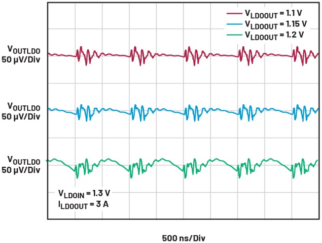
Figure 2. These scope captures are for the circuit in Figure 3 and show the PSRR caused noise is worse for the higher LDO output voltages.
Now consider the advantage that VIOC offers compared to the examples shown in figures 2 and 3. The VIOC system shown in the circuit of Figure 1 maintains a consistent input-to-output voltage for the LDO as the LDO output is varied to keep the noise-minimizing PSRR high. Because the switching regulator output voltage self-adjusts lower if the LDO output decreases and self-adjusts higher if the LDO output increases, the noise caused by the switcher’s output voltage ripple at the LDO’s output remains at a low level as the LDO’s output voltage is varied to three different levels, as shown in Figure 4.
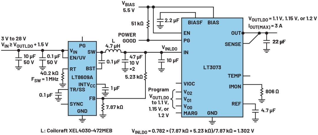
Figure 3. This circuit does not use VIOC.
The Benefit of VIOC on Efficiency, Protection, and Operation
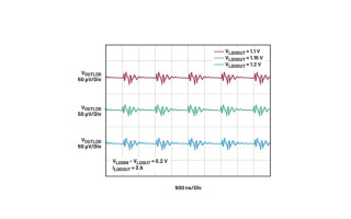
In addition to the noise-minimizing, high PSRR benefit, a system with VIOC consistently maintains an optimal input-to-output voltage for operation that is efficient, protected, and highly capable. The benefit to efficiency is clear because when the LDO output voltage decreases while the LDO input voltage remains constant as in the Figure 3 circuit, the power dissipation in the LDO increases and the efficiency decreases. For the VIOC system in Figure 1, the power dissipation remains constant because VIOC maintains a constant input-to-output voltage for the LDO even as the LDO output varies.
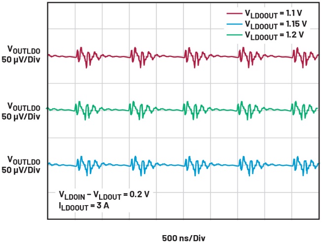
Figure 4. These scope captures are for the circuit in Figure 1 showing the PSRR caused noise is consistently low because the circuit maintains a constant input-to-output voltage for the LDO.
Also, certain conditions and faults in systems that do not use VIOC can cause the LDO input-to-output voltage to increase to undesirable amounts. For example, the LDO input-to-output voltage can increase too much if both the switching regulator output and LDO output are programmed to relatively high voltages and there is a shorted-output fault on the LDO. A shorted-output fault on the LDO will cause a high input-to-output voltage across the LDO since there is no VIOC to force the switching regulator output voltage to decrease and maintain a programmed LDO input-to-output voltage. The high LDO input-to-output voltage during the fault when the LDO output is shorted can increase power dissipation in the LDO so much that the LDO may exceed its recommended operating temperature, which may reduce reliability.
The high LDO input-to-output voltage during the fault when the LDO output is shorted can also prevent the LDO from recovering properly when the shorted output fault is removed because many high voltage LDOs have a protection feature called current-limit foldback.
Current-limit foldback is a protection technique used in power supplies and voltage regulators to reduce the output current when an overcurrent or short-circuit condition occurs. Unlike simple current limiting, which maintains a constant current during a fault, foldback current limiting decreases both the output voltage and current, thereby reducing the power dissipation in the circuit components. This helps protect the power supply and connected devices from damage due to excessive heat and current.1
Figure 5 shows the typical current-limit foldback for the LT3041 LDO. Note in Figure 5 that the LDO is capable of less output current for input-to-output voltages that are greater than 11 V. Many of the data sheets for LDOs from ADI include a section called Overload Recovery that explains why current-limit foldback can prevent an LDO that is programmed to a relatively high output voltage with a relatively high load from recovering to the correct output voltage when the short is removed on the LDO output.
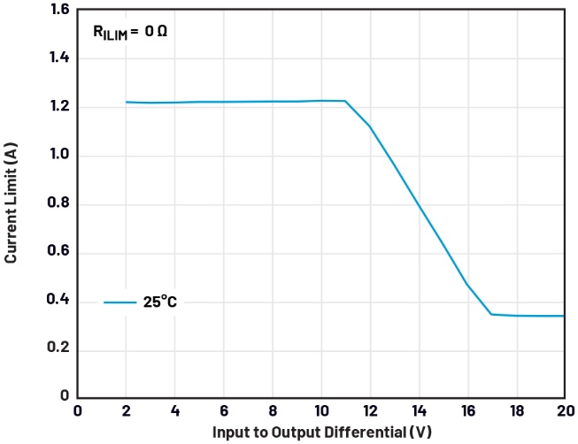
Figure 5. The typical current-limit foldback for the LT3041 LDO.
Current-limit foldback in circuits without VIOC can also prevent proper startup for high voltage circuits because an LDO’s output voltage is initially zero volts when turn-on occurs before the output voltage ramps up to the desired output regulation voltage during normal operation. If the input voltage is relatively high at turn-on, current-limit foldback may limit the LDO current too much and prevent the LDO output voltage from ramping to the desired regulation voltage. VIOC automatically maintains the correct switching regulator output voltage and consequently the correct LDO input-to-output voltage to ensure proper operation in both the fault and startup cases.
Conclusion
Part 1 of this series has laid the foundation for understanding how to design efficient, low-noise power systems using VIOC-enabled LDOs in combination with buck regulators—the most prevalent configuration in modern applications. The article also explored recommended LDO-switching regulator pairings and the rationale behind them to show how thoughtful component selection can significantly enhance system performance. The article demonstrated how leveraging the VIOC feature can reduce output noise, improve thermal efficiency, and bolster system protection and performance during startup and overload recovery.
Part 2 of this article explores how these devices maintain a constant input-to-output voltage differential and provides practical tools to simplify VIOC system implementation.
Reference
1T.K. Hareendran. “Foldback Current Limiting - Little Secrets.” Codrey, November 2021.
Andrew Radosevich is a senior manager with Analog Devices and, after being a product applications engineer for switching regulators and linear regulators for many years, now leads a team that provides that support. Andrew received an M.S.E.E. from San Jose State University, specializing in power electronics.
Matt Grobelny has been a product marketing manager for LDO and monolithic boost converters at Analog Devices since 2024. He holds a Master of Engineering in VLSI systems from the University of Limerick and in optoelectronics from Wroclaw University of Science and Technology. Matt brings many years of hands-on experience as an evaluation and applications engineer, specializing in switching regulators and optical laser drives.