System-on-Chip (SoC) Design- and Development Considerations ? Part 1
March 20, 2019
Story

Design of a control module based on the Arria 10 SoC for use in a medical application.
The design team of HEITEC, an independent provider of electronic design services, was commissioned by a customer to develop a highly performing controller module that manages the actual devices of the application that control the diagnostic medical imaging and safety-critical processes, and that handles all necessary interfaces to the peripherals and a GUI PC. The challenge was to implement a lot of functionality in compressed space with great efficiency. For the design, an Intel (Altera) Arria 10 SoC (System-On-Chip) building block was selected, that combines a dual-core ARM Cortex-A9 processor with programmable FPGA logic.
This article outlines the project and the experiences gained during the design process. The alternative options of available SoCs from different providers are compared and the key factors of the selection are explained. This process led to the current solution, which includes both hardware and software aspects.
Finally, it is shown that such a design can be used not only for the individual requirements of the actual project, but that it is also transferable to a variety of other sophisticated high-performance applications in the industrial control, communication or test and measurement areas.
In addition to an embedded CPU, the application also includes an FPGA. At the beginning of the FPGA design process, the decision had to be made why a system-on-chip should be used, despite the expectable higher investment. The technical advantages had to prevail in order to justify the initially higher price. SoC building blocks with FPGA integrate a processor core and FPGA architecture in one device. For some time now, technological progress has allowed for integrating these two functionalities into one chip, providing an attractive solution for forward-looking designs. In the selected single chip solution, CPU and FPGA have access to the storage via the same interface featuring DMA (Direct Memory Access). This results in multiple advantages such as greater design flexibility, a higher level of integration with fewer components, an easier to manage solution with only one device, the coupling of processor and FPGA as well as a high-performance internal bus interface between CPU and programmable FPGA logic.
Direct storage access leads to faster data transmission, while simultaneously relieving the processor. The FPGA design enables hardware-controlled access, even without a local bus. SoCs also offer a lot of expansion capability in order to integrate required functionalities tailored to the respective task. The integration of specific software algorithms into the hardware with filter algorithms as well as the possibility of specific calculations were other reasons for the decision. Standard software is also very well usable along with the ARM processor part of the chosen SoC. Through the compact design and through avoiding additional components, better thermal control is feasible, as only one component needs to be cooled. The conflict between performance and energy efficiency was thus best addressed by an SoC. In consequence, this setup with lower energy consumption results in better overall performance with more possibilities for miniaturization, longer product life and availability, as well as significant cost reduction.
The next decision-making step was to select the SoC from all the solutions available on the market. After reviewing the required properties, Xilinx and Intel's specific application SoCs were up for discussion. These two main FPGA providers have SoC FPGA families with a similar approach – a standard ARM Cortex-A9 processor dual core as a hard macro - in the portfolio. Both solutions rely on a dedicated, "hardened" processor subsystem with a fully equipped ARM Cortex-A9 processor including a complete storage hierarchy and associated peripheral building blocks that boot and work like a normal ARM processor. So far, the two concepts are very similar, but the Xilinx Zynq does not support ECC (Error Correcting Code) in the processor caches and in the on-chip processor RAM.
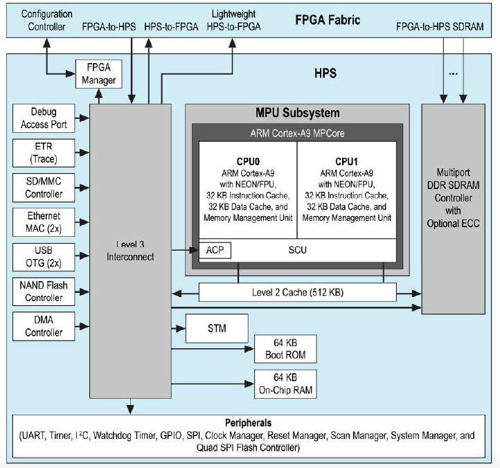
However, given the system requirements of the application, the fully supported ECC functionality was ultimately the key to the HEITEC developer team's decision to deploy the 20nm processor technology-based Intel Arria 10 SoC. This consists of the Hard Processor System (HPS for short) and a separate FPGA part, which are connected to a bridge for high data throughput, allowing for significantly faster access than the usual PCI latency. Combined hardware and software processing are possible this way. The common HPS/FPGA bridge is equipped with an intelligent scheduler to the DDR interface.
In addition to the Dual Core ARM processor, important features of the Arria 10 SoC include a 7500 MIPS architecture at a processor frequency of 1.5 GHz, L1 cache with 32 KB for data processing and command input, a 512 KB L2 cache with ECC, on-chip processor 256KB RAM with ECC, HPS-external DDR3 storage interface with 533 MHz, 32 Bit data + 8 bit ECC. The extensive processor peripherals include a Quad SPI Flash controller, NAND Flash Controller for higher data throughput, three 10M/100M/1G Ethernet controllers, two USB 2.0-On-The-Go controllers, 1 SD/MMC/SDIO controller, UART 16550, five I2C controllers, two SPI master and slave controllers each, as well as four 32-bit watchdog timers. In addition, 270K logic elements, up to three hardened memory controllers with ECC as well as error correction (ECC) and storage protection are implemented in the selected model. The safe boot order is free to choose: Either the processor first or the FPGA first or both at the same time. The packaging is a 780-Pin FineLine Ball-Grid Array (FBGA)with 1.0 mm ball pitch.
Thus, the Intel Arria 10 SoC provides a processor with a large functional scope for embedded peripherals, hardened floating point DSP blocks, embedded high-speed transceivers, hard memory controllers and protocol of (IP) controllers. All the required interfaces are already on the building block, ergo, all in all an ideal highly integrated package designed for design productivity. With its set-up, it is the optimal combination for medium-sized applications and the requirements of the target application.
This blog is Part 1 in a series of 3, click here for Part 2 and Part 3.
Roland Chochoiek
Executive VP Electronics HEITEC AG
Roland holds degrees in Electronics and Business Administration and worked in a number of senior management positions within the high-tech industry, including Force Computers, Solectron and Rittal. Since 2010 he has been the Executive Vice President of the Electronics Business Unit of HEITEC AG.