High Speed PCB Design Precautions to Reduce EMI
June 10, 2020
Story
This document is written based on the practical observation of electromagnetic interference from high-speed signals and power switchers, which can cause failure in the certification process.
This document is written based on the practical observation of electromagnetic interference from high-speed signals and power switchers, which can cause failure in the certification process. Layout and schematic design recommendation for the components used in the product might be available in the datasheets, but practical observation and solution to it may be different.
This document covers high-speed signals like HDMI, MIPI CSI, MIPI DSI, and Ethernet. Radiation in the frequency range above 9 kHz should be within set limits by certification standards. Radiation from the device is generally multiple harmonics of the high frequency clock present at PCB. Single ended clock radiated more compared to differential clock as voltage levels and power are higher for single ended signals. It is highly recommended to use series 0 Ohm Resistor provision at the source side of any high-speed single ended clock.
During certification, increasing series resistor value can help in controlling the overshoot and undershoot present in the clock, which is the main cause of radiation. The increasing the value of series Resistor helps to reduce overshoot and undershoot. The maximum value of the series termination resistor can be determined by setup and hold time violation of the receiver. It is also advisable not to use duplicated frequency wherever possible.
For example, if two switcher parts are used as a power supply regulator, then make sure that both do not operate on the same switching frequency as radiation will sum up which can exceed the prohibited limits of radiation. Higher length of clock signal cause an increase in radiation power. For example, longer HDMI cable will act as Antenna so that radiation of the HDMI interface will be higher in this case.
Layout plays an important role in the radiation. Make sure that the clock signal is designed to meet the characteristic impedance requirement and continuous grounding provided around clock traces so that impedance miss-match can be avoided. Follow the layout guideline of chip manufacturer very accurately and make sure that schematic and layout for that particular section reviewed by the manufacturer with a radiation perspective. Chip manufacturer might have some suggestions to add to the new design as per their experience with certification failures related to the chip.
1. HDMI (High-Definition Multimedia Interface)
EMI failure due to HDMI Interface is most common in the embedded products. HDMI radiation appears on fundamental and usually up to fifth harmonics at 148.5MHz, 297MHz, 445.5MHz, 594MHz, 742.5MHz, and 891MHz.
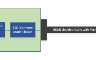
The source of radiation could be from HDMI cable, PCB design, or display itself if not certified. The common mode choke and termination resistors/capacitors shall help to remove radiation from PCB but the common mistake happens with HDMI cable selection. Different cables from the different manufacturer provides a different level of emission and even if they are shielded. Therefore, it is very important that cable selected from trusted vendor like Molex or TE. Of course the selected cable should be shielded and have inbuilt ferrite core. It is recommended that 3-4 different cables (From different make) should be carried for the pre-scan to verify the performance with each of them.

The below techniques can help reduce the radiation from HDMI signals:
- The common mode choke should be selected with the cutoff frequency 5-6 times higher than the fundamental frequency. In the case of 148.5MHz, more than 1GHz cut-off frequency shall be ideal.
- Differential signals passing from one layer to another should make sure that the ground via located adjacent to the signals to reduce the loop inductance.
- In the case of HDI PCB, ground via should transit down as signal to flow back to the source in the shortest path.
- The metal enclosure should take advantage of a good earthing scheme with cable shields appropriately terminated with the enclosure using shielded connectors to reduce the interference.
- Stitching capacitors recommended in the case of reference plane with different potentials (ground and power).
- Other general guidelines like length matching (10mil intra-pair and 100mil inter-pair), impedance matching (100 Ohm), solid reference plane, micro-strip routing, less number of vias, 45deg bends are best practices followed.
2. MIPI DSI and CSI (Mobile Industry Processor Interface)
MIPI signals (CSI/DSI) are specially designed for the mobile industry, so they are very low power differential signals, and less likely to radiate. MIPI signal clock varies depending on the resolution parameters.
Radiation could be possible on the FPC cables carrying MIPI signals. In the case of custom cable, we’re adding shield or ground on both sides can instantly help but it may affect the flexibility of the cable. The best way is to use the hatched ground on the immediate layer as reference ground. Off-course common mode choke with higher bandwidth will help remove the common mode noise from the PCB. MIPI signals have a data rate of 80Mbps-2.5Gbps for D-PHY and 183Mbps -5.7Gbps for C-PHY. Therefore, it is very important to provide a guar ring and at least 40-mil isolation from other signals.

The below techniques can help reduce the radiation from the MIPI signals:
- Select the common mode choke with more than 2GHz cut-off frequency for D-PHY. Special filters are available for C-PHY to pass the trio signals.
- Differential signals passing from one layer to another should make sure that the ground via located adjacent to the signals to reduce the loop inductance.
- In the case of HDI PCB, ground via should transit down as signal to flow back to the source in the shortest path.
- In the case of EMI film on the FPC, make sure the ends of the film connected to exposed signal ground on FPC.
- Stitching capacitors recommended in the case of reference plane with different potentials (ground and power).
- Other general guidelines like length matching (25-mil intra-pair and 55-mil inter-pair), impedance matching (100 Ohm/85 ohm in few cases), solid reference plane, micro-strip routing, less numbers of vias, 45deg bends are best practices followed.
3. Ethernet
Radiation on Ethernet signal is directly proportional to the length of the twisted pair cable. Shielded CAT5 cables and ferrite core on the cable will help in reducing the interference.
Differential MDI signal radiates when common mode noise present on the cable returns the noise through chassis ground.
Noise from single ended MII and power section can be coupled to the twisted cable through chassis ground can produce unwanted radiations.
The below techniques can help reduce the radiation from the Ethernet signals:
- Ferrite core on Ethernet cable can reduce EMI. Keep the different type of CAT5 cables during the certification process.
- MDI signal should be well isolated from MII signals (min 40 mils apart).
- Maintain minimum length for the single ended MII signals.
- Void should be maintained below the magnetic component throughout all the layers.
- MDI and MII signals passing from one layer to another should make sure that the ground via located adjacent to the signals to reduce the loop inductance.
- In the case of HDI PCB, ground via should transit down as signal to flow back to the source in the shortest path.
- The metal enclosure should take advantage of a good earthing scheme with cable shields appropriately terminated with the enclosure using shielded RJ 45 connectors to reduce the interference.
- Stitching capacitors recommended in the case of reference plane with different potentials (ground and power).
- Other general guidelines like length matching (10mil intra-pair and 100mil inter-pair), impedance matching (100 Ohm), solid reference plane, micro-strip routing, less numbers of vias, 45deg bends are best practices followed.
4. DC-DC Power supply generation
For high-speed PCB design, the noisy power supply is one of the major contributors to EMI-EMC radiation. Steady and less noisy power will surely help to reduce the EMI.
Processor, memory, and bridge chip used for high-speed interfaces work on very low voltage. DC-DC Switching regulators are selected in design to get high output current and efficiency. But switching frequency, ripple (overshoot and undershoot) noise generated from these switchers contribute to the radiation. Coupling of noisy signals in the ground can increase radiation as the ground will travel along with cables, which can act as an antenna for high frequency noise.
If system actual power consumption is higher (>10W) and longer length cables are involved in the product then it is recommended to use common mode choke and LC filtering at the input DC supply. Online calculators are available to calculate L and C values for a particular frequency for which radiated power needs to be attenuated. A higher value of the inductor is preferred is there are no constraints in the space.

Generally, high frequency (ringing) observed at overshoot and undershoot of switching frequency is more likely to radiate.

Snubber tuning will help to reduce this overshoot and undershoot power. Use bigger packages or high power rated resistors as high frequency noise will be bypassed through it and the smaller packages might increase the temperature of PCB. Snubber circuit should be installed at the switching node of the inductor.

Points to remember for high speed PCB Design
· The surface mount part should be preferred against the through-hole part. Through-hole parts like the capacitor becomes more inductive above 80MHz, which might cause radiation/sorting issues at a higher frequency.
· Keep high-speed signal traces as small as possible and provide grounding as much as possible to reduce loop inductance.
· Try to avoid adjacent signal layers in stack-ups or use orthogonal routing to reduce capacitive coupling.
· Place decoupling capacitors very close to IC pins. This will help in quicker switching between power and ground.
· Use star routing for the signals and single point routing for the power.
· Use Ferrite Beads on Power supply output. Placing capacitor around the ferrite bead will act as low pass filter for high frequency noise.
· Keep 0E series termination resistor provision at every clock output which is >1MHz. It will help to tune in case of interference issues.
· For crystal, select a parallel capacitor considering load and stray capacitance as per the datasheet. They are a fundamental source of radiation so follow IC recommendation for crystal routing. Also, try to keep crystal/oscillators at the center of the PCB and not at the edges.
· Traces at the edge of the PCB should not be routed with 90-degree angle.
· Keep shield provision for the RF section. It is mandatory for the FCC (For Modular certification).
· High frequency square wave is made of multiple high frequency sine waves. So, make sure that this type of critical signal should have proper grounding around it.
· Make sure for the continuous ground plane that vias should not make islands that are connected with a very thin copper area. This can increase the ground return path for the signals.
· FR4 material is best with <5Gbps clock speed and at low cost. For higher than 5Gbps use other materials like Nelco, Megatron, Rogers.
· Keep >3W spacing of other signals from high speed signals

· The power layer should be well inside the PCB edge compared to ground layer. As per thumb rule, 20H is preferable. (H=Dielectric thickness between layers)

Summary
This document is based on practical observations of EMI reduction at high-speed PCB designs. EMI precautions are very helpful for the certification. Radiation of high speed interfaces varies from design to design so it is recommended to use provisions in design that will help in tuning during the certification process.
This document covers precautions for high speed signals used commonly across PCBs. EMI issue due to the HDMI interface is observed in almost all the products. Series, parallel termination, chokes do not help much to reduce radiation. Change in the HDMI cable and HDMI display changes the radiation power. Long cables will act as an antenna for the high speed interfaces so lots of precautions need to be taken if the product has multiple long cables connected to it (For example, Automotive product).
eInfochips, an Arrow company, is a leading global provider of product engineering and semiconductor design services. For more information on PCB design solutions please connect us today.

Divyesh Patel possesses a wealth of experience in successfully resolving various certification-related issues across multiple products. Furthermore, he has a proven track record in the end-to-end design of high-speed embedded PCBAs, starting from the architectural phase through to production.”