More KiCad Layout Quick Tips and Techniques
December 20, 2021
Blog
When I was first introduced to KiCad, routing traces was described as a bit of an art, something to be learned from experience. I’d say that is true, however, in addition to my first quick tips article, here are some additional–perhaps more strategic–techniques that I can offer to those getting started.
Don’t Fear Vias
While vias can certainly be overused, in many designs they are both necessary and a great alternative to running a very long trace. If you have the choice between snaking a signal line around and around to get to its destination, and hitting v to route it between layers, you know what to do. Of course, if there’s a way to simplify your design so that neither is necessary, all the better.
Firmware IO organization
If you have a series of, say 6 input buttons, it only makes sense to assign them in a logical order with respect to your microcontroller. Perhaps pin 1 goes to the button on the top left, pin 2 next to that, all the way down to pin 6, maybe on the bottom-right if it’s in a small keypad arrangement. However, what if this arrangement means that you need to snake signal lines back and forth, and/or use a significant number of vias?
If there’s a more direct connection arrangement for IO pins, you might instead consider changing things around in the Schematic Layout Editor to match the physical situation, rather than pin numbers. IO can then be assigned programmatically. This type of firmware assignment is generally trivial, so if it saves you hassle and/or board space, it may be well worth it.
Redesign When Needed


Caption: JC Pro Macro 2 board routing in August (top), current routing with Pro Micro board mounting flipped and other changes (bottom)
Image Credit: screencap
During the development of my JC Pro Macro 2 Kickstarter project, I went through roughly five iterations of the board (not counting the original JC Pro Macro device). Each time I thought I had the design just right, and to my credit each one nominally worked. However, there were iterative improvements that needed to be made to push toward excellence. Tearing up tracks on-screen is a bit nerve-racking, but in the end I think it was worth it.
One rather major revision was flipping the orientation of the Pro Micro board. This meant that the headers didn’t have to be mounted on top, a bit of a holdover from the way the JC Pro Macro board was originally designed, which would have likely led to confusion and sub-optimal usability.

Image Credit: screencap
Flipping things wasn’t as hard as I thought, and I think it will be well worth it in the long term. If you’re not sure about something, you can always archive your project to allow you to go back to a known good state.
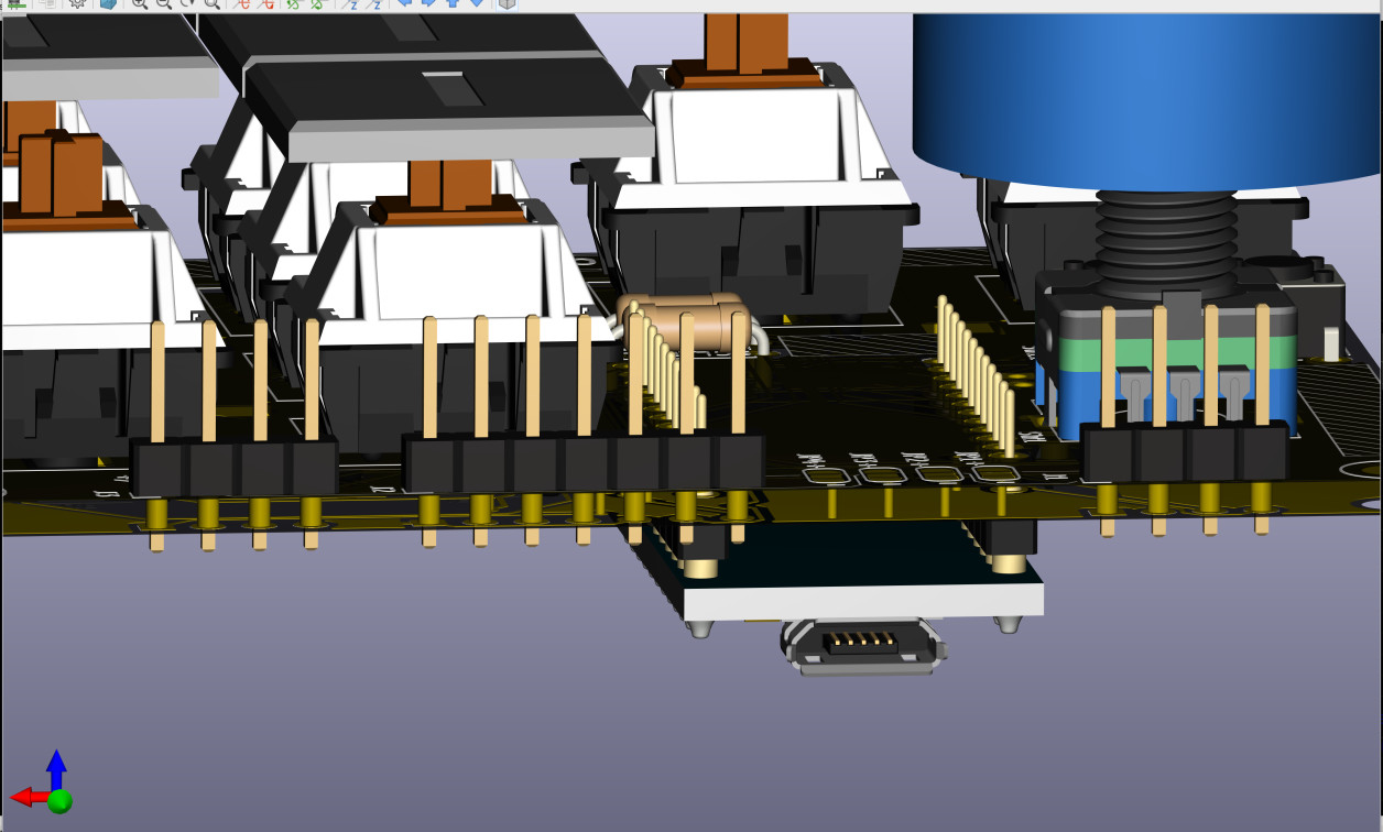
Visualization

Image Credit: screencap
In KiCad’s Pcbnew layout tool, there are three main options on the sidebar for how to display your design-in-progress. I tend to leave the middle, “Do not show filled areas in zones,” as my default, as it gives good visibility of traces in multiple layers. When you need to visualize filled areas, the icon just above that shows a more complete picture of the board, including signal lines and copper pours. The down side is that lower layers will often be obscured, and you’ll need to be more selective about which layers are shown. However, this can be an important tool for tracking down pesky ratsnest elements that remain unconnected.
Finally, taking a look at your board/assembly on the 3D Viewer, especially with “Show board body” turned off, and possibly the 3D models as well, under Preferences > Display Options can be instructive. If nothing else, a quick look in the 3D viewer can provide a little reassurance of how things will look before you send it off for fabrication!
Jeremy Cook is a freelance tech journalist and engineering consultant with over 10 years of factory automation experience. An avid maker and experimenter, you can follow him on Twitter, or see his electromechanical exploits on the Jeremy Cook YouTube Channel!